7 input capture register 1 - icr1h and icr1l, 8 timer/counter1 interrupt mask register - timsk1 – Rainbow Electronics ATmega64C1 User Manual
Page 132

132
7647A–AVR–02/08
ATmega32/64/M1/C1
13.10.7
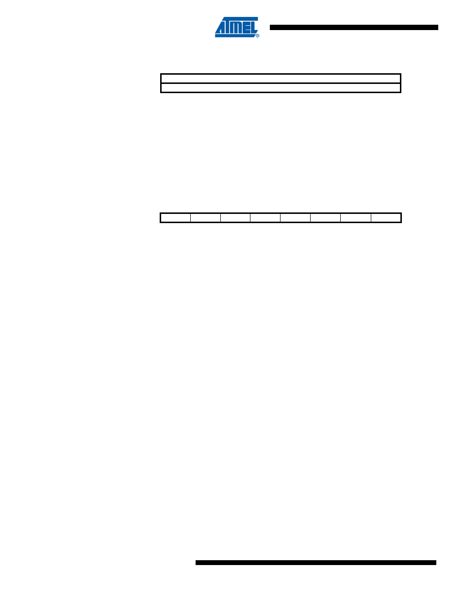
Input Capture Register 1 – ICR1H and ICR1L
The Input Capture is updated with the counter (TCNTn) value each time an event occurs on the
ICPn pin (or optionally on the Analog Comparator output for Timer/Counter1). The Input Capture
can be used for defining the counter TOP value.
The Input Capture Register is 16-bit in size. To ensure that both the high and low bytes are read
simultaneously when the CPU accesses these registers, the access is performed using an 8-bit
temporary High Byte Register (TEMP). This temporary register is shared by all the other 16-bit
registers.
See “Accessing 16-bit Registers” on page 108.
13.10.8
Timer/Counter1 Interrupt Mask Register – TIMSK1
• Bit 7, 6 – Res: Reserved Bits
These bits are unused bits in the ATmega32/64/M1/C1, and will always read as zero.
• Bit 5 – ICIE1: Timer/Counter1, Input Capture Interrupt Enable
When this bit is written to one, and the I-flag in the Status Register is set (interrupts globally
enabled), the Timer/Counter1 Input Capture interrupt is enabled. The corresponding Interrupt
Vector (
see “Reset and Interrupt Vectors Placement in AT90PWM324
(1)
” on page 54
) is exe-
cuted when the ICF1 Flag, located in TIFR1, is set.
• Bit 4, 3 – Res: Reserved Bits
These bits are unused bits in the ATmega32/64/M1/C1, and will always read as zero.
• Bit 2 – OCIE1B: Timer/Counter1, Output Compare B Match Interrupt Enable
When this bit is written to one, and the I-flag in the Status Register is set (interrupts globally
enabled), the Timer/Counter1 Output Compare B Match interrupt is enabled. The corresponding
Interrupt Vector (
see “Reset and Interrupt Vectors Placement in AT90PWM324
(1)
” on page 54
) is
executed when the OCF1B Flag, located in TIFR1, is set.
• Bit 1 – OCIE1A: Timer/Counter1, Output Compare A Match Interrupt Enable
When this bit is written to one, and the I-flag in the Status Register is set (interrupts globally
enabled), the Timer/Counter1 Output Compare A Match interrupt is enabled. The corresponding
Interrupt Vector (
see “Reset and Interrupt Vectors Placement in AT90PWM324
(1)
” on page 54
) is
executed when the OCF1A Flag, located in TIFR1, is set.
• Bit 0 – TOIE1: Timer/Counter1, Overflow Interrupt Enable
When this bit is written to one, and the I-flag in the Status Register is set (interrupts globally
enabled), the Timer/Counter1 Overflow interrupt is enabled. The corresponding Interrupt Vector
(
see “Reset and Interrupt Vectors Placement in AT90PWM324
(1)
” on page 54
) is executed when
the TOV1 Flag, located in TIFR1, is set.
Bit
7
6
5
4
3
2
1
0
ICR1[15:8]
ICR1H
ICR1[7:0]
ICR1L
Read/Write
R/W
R/W
R/W
R/W
R/W
R/W
R/W
R/W
Initial Value
0
0
0
0
0
0
0
0
Bit
7
6
5
4
3
2
1
0
–
–
ICIE1
–
–
OCIE1B
OCIE1A
TOIE1
TIMSK1
Read/Write
R
R
R/W
R
R
R/W
R/W
R/W
Initial Value
0
0
0
0
0
0
0
0
