10 16-bit timer/counter register description, 1 timer/counter1 control register a - tccr1a, Figure 13-12 – Rainbow Electronics ATmega64C1 User Manual
Page 126
126
7647A–AVR–02/08
ATmega32/64/M1/C1
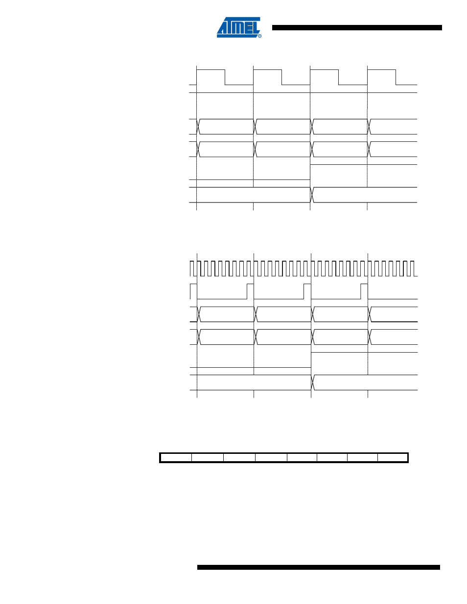
Figure 13-12. Timer/Counter Timing Diagram, no Prescaling
shows the same timing data, but with the prescaler enabled.
Figure 13-13. Timer/Counter Timing Diagram, with Prescaler (f
clk_I/O
/8)
13.10 16-bit Timer/Counter Register Description
13.10.1
Timer/Counter1 Control Register A – TCCR1A
• Bit 7:6 – COMnA1:0: Compare Output Mode for Channel A
• Bit 5:4 – COMnB1:0: Compare Output Mode for Channel B
The COMnA1:0 and COMnB1:0 control the Output Compare pins (OCnA and OCnB respec-
tively) behavior. If one or both of the COMnA1:0 bits are written to one, the OCnA output
overrides the normal port functionality of the I/O pin it is connected to. If one or both of the
COMnB1:0 bit are written to one, the OCnB output overrides the normal port functionality of the
TOVn
(FPWM)
and ICFn
(if used
as TOP)
OCRnx
(Update at TOP)
TCNTn
(CTC and FPWM)
TCNTn
(PC and PFC PWM)
TOP - 1
TOP
TOP - 1
TOP - 2
Old OCRnx Value
New OCRnx Value
TOP - 1
TOP
BOTTOM
BOTTOM + 1
clk
Tn
(clk
I/O
/1)
clk
I/O
TOVn
(FPWM)
and ICF n
(if used
as TOP)
OCRnx
(Update at TOP)
TCNTn
(CTC and FPWM)
TCNTn
(PC and PFC PWM)
TOP - 1
TOP
TOP - 1
TOP - 2
Old OCRnx Value
New OCRnx Value
TOP - 1
TOP
BOTTOM
BOTTOM + 1
clk
I/O
clk
Tn
(clk
I/O
/8)
Bit
7
6
5
4
3
2
1
0
COM1A1
COM1A0
COM1B1
COM1B0
–
–
WGM11
WGM10
TCCR1A
Read/Write
R/W
R/W
R/W
R/W
R
R
R/W
R/W
Initial Value
0
0
0
0
0
0
0
0