Atmega32/64/m1/c1 typical characteristics – Rainbow Electronics ATmega64C1 User Manual
Page 320
320
7647A–AVR–02/08
ATmega32/64/M1/C1
Notes:
1. t
WLRH
is valid for the Write Flash, Write EEPROM, Write Fuse bits and Write Lock bits
commands.
2. t
WLRH_CE
is valid for the Chip Erase command.
26. ATmega32/64/M1/C1 Typical Characteristics
All DC characteristics contained in this datasheet are based on simulations and characterization
of similar devices in the same process and design methods. These values are preliminary repre-
senting design targets, and will be updated after characterization of actual automotive silicon
data.
The following charts show typical behavior. These figures are not tested during manufacturing.
All current consumption measurements are performed with all I/O pins configured as inputs and
with internal pull-ups enabled. A sine wave generator with rail-to-rail output is used as clock
source.
All Active- and Idle current consumption measurements are done with all bits in the PRR register
set and thus, the corresponding I/O modules are turned off. Also the Analog Comparator is dis-
abled during these measurements.
and
the additional current consumption compared to I
CC
Active and I
CC
Idle for every I/O module con-
trolled by the Power Reduction Register. See “Power Reduction Register” on page 37 for details.
The power consumption in Power-down mode is independent of clock selection.
The current consumption is a function of several factors such as: operating voltage, operating
frequency, loading of I/O pins, switching rate of I/O pins, code executed and ambient tempera-
ture. The dominating factors are operating voltage and frequency.
The current drawn from capacitive loaded pins may be estimated (for one pin) as C
L
*
V
CC
*f where
C
L
= load capacitance, V
CC
= operating voltage and f = average switching frequency of I/O pin.
The parts are characterized at frequencies higher than test limits. Parts are not guaranteed to
function properly at frequencies higher than the ordering code indicates.
The difference between current consumption in Power-down mode with Watchdog Timer
enabled and Power-down mode with Watchdog Timer disabled represents the differential cur-
rent drawn by the Watchdog Timer.
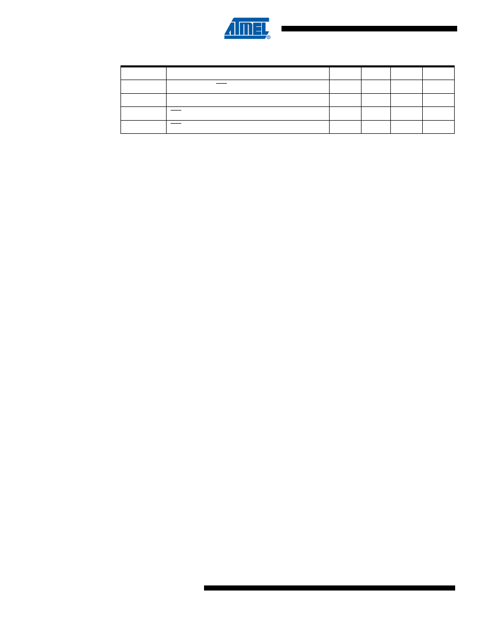
t
XLOL
XTAL1 Low to OE Low
0
ns
t
BVDV
BS1 Valid to DATA valid
0
250
ns
t
OLDV
OE Low to DATA Valid
250
ns
t
OHDZ
OE High to DATA Tri-stated
250
ns
Table 25-3.
Parallel Programming Characteristics, V
CC
= 5V ± 10% (Continued)
Symbol
Parameter
Min.
Typ.
Max.
Units