1 latching of fuses, Refer to, Table 24-7 – Rainbow Electronics ATmega64C1 User Manual
Page 292
292
7647A–AVR–02/08
ATmega32/64/M1/C1
Note:
1. See
“Alternate Functions of Port C” on page 71
for description of RSTDISBL Fuse.
2. The SPIEN Fuse is not accessible in serial programming mode.
3. See
“Watchdog Timer Configuration” on page 53
for details.
4. The default value of BOOTSZ1..0 results in maximum Boot Size. See
for details
.
Note:
1. The default value of SUT1..0 results in maximum start-up time for the default clock source.
See
for details.
2. The default setting of CKSEL3..0 results in internal RC Oscillator @ 8 MHz. See
for details.
3. The CKOUT Fuse allows the system clock to be output on PORTB0. See
for details.
4. See
“System Clock Prescaler” on page 36
for details.
The status of the Fuse bits is not affected by Chip Erase. Note that the Fuse bits are locked if
Lock bit1 (LB1) is programmed. Program the Fuse bits before programming the Lock bits.
24.3.1
Latching of Fuses
The fuse values are latched when the device enters programming mode and changes of the
fuse values will have no effect until the part leaves Programming mode. This does not apply to
Table 24-6.
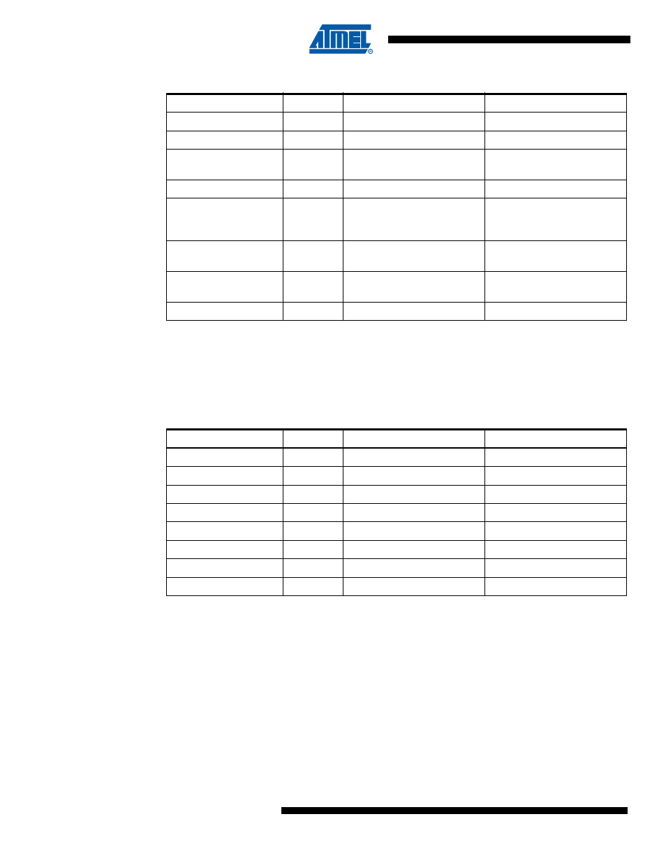
Fuse High Byte
High Fuse Byte
Bit No
Description
Default Value
7
External Reset Disable
1 (unprogrammed)
DWEN
6
debugWIRE Enable
1 (unprogrammed)
SPIEN
5
Enable Serial Program and
Data Downloading
0 (programmed, SPI
programming enabled)
WDTON
4
Watchdog Timer Always On
1 (unprogrammed)
EESAVE
3
EEPROM memory is
preserved through the Chip
Erase
1 (unprogrammed), EEPROM
not reserved
BOOTSZ1
2
Select Boot Size
(see Table 113 for details)
0 (programmed)
BOOTSZ0
1
Select Boot Size
(see Table 113 for details)
0 (programmed)
BOOTRST
0
Select Reset Vector
1 (unprogrammed)
Table 24-7.
Fuse Low Byte
Low Fuse Byte
Bit No
Description
Default Value
7
Divide clock by 8
0 (programmed)
CKOUT
6
Clock output
1 (unprogrammed)
SUT1
5
Select start-up time
1 (unprogrammed)
SUT0
4
Select start-up time
0 (programmed)
CKSEL3
3
Select Clock source
0 (programmed)
CKSEL2
2
Select Clock source
0 (programmed)
CKSEL1
1
Select Clock source
1 (unprogrammed)
CKSEL0
0
Select Clock source
0 (programmed)