1 adlar = 0, 2 adlar = 1, 5 digital input disable register 0 - didr0 – Rainbow Electronics ATmega64C1 User Manual
Page 246: 6 digital input disable register 1- didr1
246
7647A–AVR–02/08
ATmega32/64/M1/C1
Nevertheless, to work easily with only 8-bit precision, there is the possibility to left adjust the
result thanks to the ADLAR bit in the ADCSRA register. Like this, it is sufficient to only read
ADCH to have the conversion result.
18.9.4.1
ADLAR = 0
18.9.4.2
ADLAR = 1
18.9.5
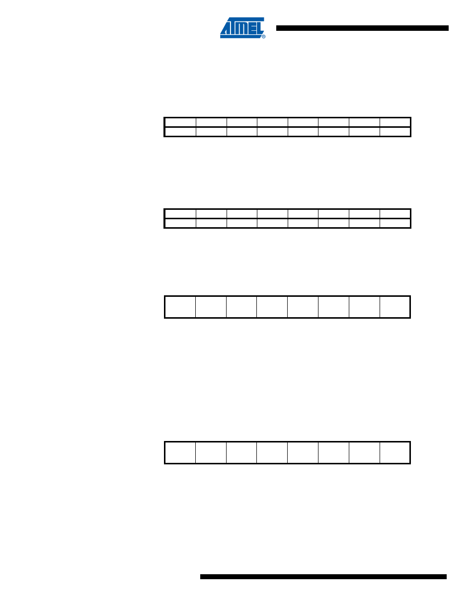
Digital Input Disable Register 0 – DIDR0
• Bit 7:0 – ADC7D..ADC0D, ACMPN0D, ACMPN1D, ACMPN2D, ACMPN3D, ACMP2D,
AMP2ND:
ADC7:0, ACMPN0, ACMPN1, ACMPN2, ACMPN3, ACMP2, AMP2N Digital Input Disable
When this bit is written logic one, the digital input buffer on the corresponding ADC pin is dis-
abled. The corresponding PIN Register bit will always read as zero when this bit is set. When an
analog signal is applied to the ADC7..0 pin and the digital input from this pin is not needed, this
bit should be written logic one to reduce power consumption in the digital input buffer.
18.9.6
Digital Input Disable Register 1– DIDR1
• Bit 6:0 – ADC10D..8D, ACMP0D, ACMP1D, ACMP3D, AMP0PD, AMP0ND, AMP1PD,
AMP1ND, AMP2PD:
ADC10..8, ACMP0, ACMP1, ACMP3, AMP0P, AMP0N, AMP1P, AMP1N, AMP2P Digital
Input Disable
When this bit is written logic one, the digital input buffer on the corresponding ADC pin is dis-
abled. The corresponding PIN Register bit will always read as zero when this bit is set. When an
Bit
7
6
5
4
3
2
1
0
-
-
-
-
-
-
ADC9
ADC8
ADCH
ADC7
ADC6
ADC5
ADC4
ADC3
ADC2
ADC1
ADC0
ADCL
Read/Write
R
R
R
R
R
R
R
R
R
R
R
R
R
R
R
R
Initial Value
0
0
0
0
0
0
0
0
0
0
0
0
0
0
0
0
Bit
7
6
5
4
3
2
1
0
ADC9
ADC8
ADC7
ADC6
ADC5
ADC4
ADC3
ADC2
ADCH
ADC1
ADC0
-
-
-
-
-
-
ADCL
Read/Write
R
R
R
R
R
R
R
R
R
R
R
R
R
R
R
R
Initial Value
0
0
0
0
0
0
0
0
0
0
0
0
0
0
0
0
Bit
7
6
5
4
3
2
1
0
ADC7D
ADC6D
ACMPN1D
AMP2ND
ADC5D
ACMPN0D
ADC4D
ADC3D
ACMPN2D
ADC2D
ACMP2D
ADC1D
ADC0D
ACMPN3D
DIDR0
Read/Write
R/W
R/W
R/W
R/W
R/W
R/W
R/W
R/W
Initial Value
0
0
0
0
0
0
0
0
Bit
7
6
5
4
3
2
1
0
-
AMP2PD
ACMP0D
AMP0PD
AMP0ND
ADC10D
ACMP1D
ADC9D
AMP1PD
ACMP3D
ADC8D
AMP1ND
DIDR1
Read/Write
-
-
R/W
R/W
R/W
R/W
R/W
R/W
Initial Value
0
0
0
0
0
0
0
0