2 adc control and status register a - adcsra, See “adc input channel – Rainbow Electronics ATmega64C1 User Manual
Page 243

243
7647A–AVR–02/08
ATmega32/64/M1/C1
• Bit 4, 2, 1, 0 – MUX4, MUX3, MUX2, MUX1, MUX0: ADC Channel Selection Bits
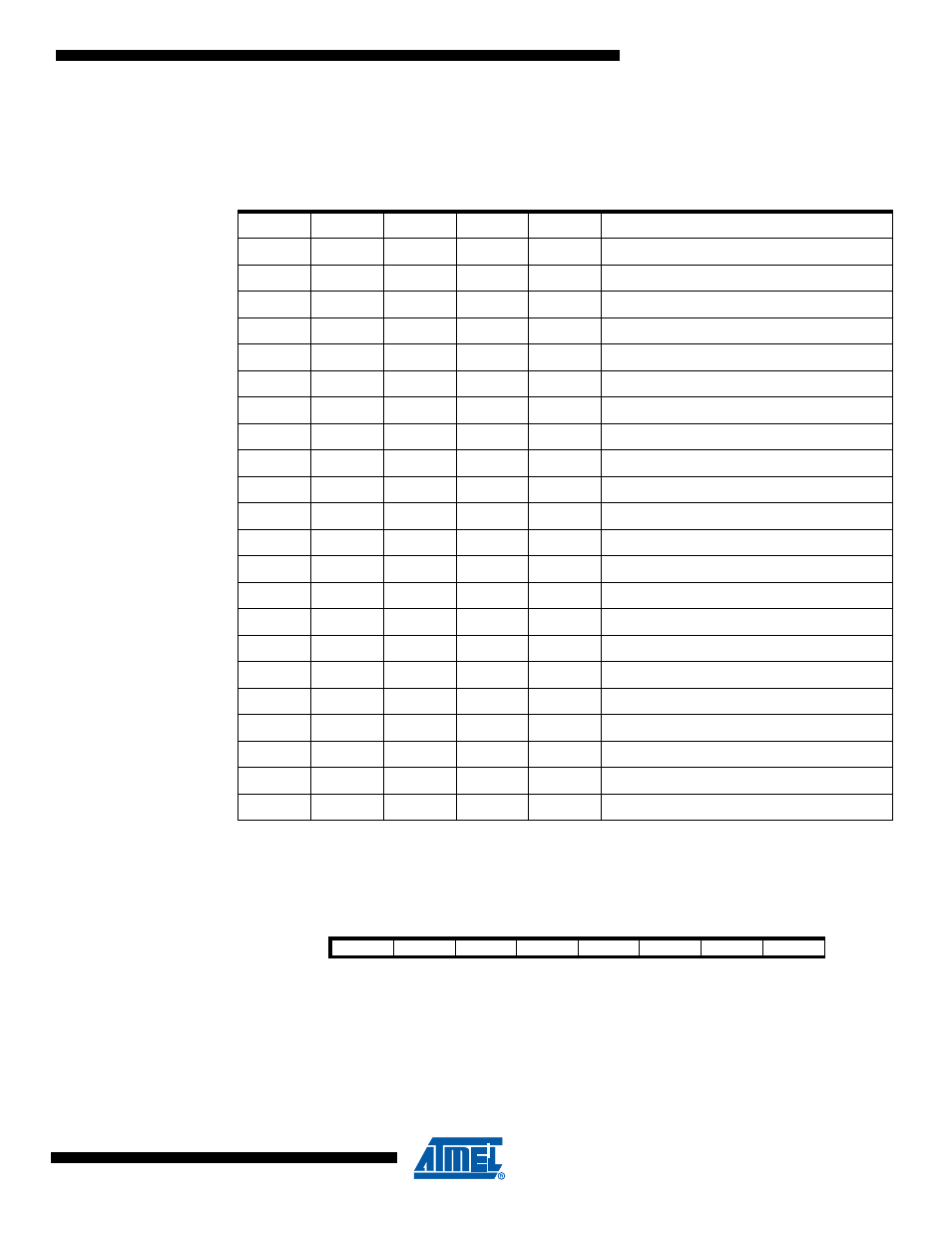
These 4 bits determine which analog inputs are connected to the ADC input. The different set-
ting are shown in
.
If these bits are changed during a conversion, the change will not take effect until this conversion
is complete (it means while the ADIF bit in ADCSRA register is set).
18.9.2
ADC Control and Status Register A – ADCSRA
• Bit 7 – ADEN: ADC Enable Bit
Set this bit to enable the ADC.
Clear this bit to disable the ADC.
Clearing this bit while a conversion is running will take effect at the end of the conversion.
Table 18-5.
ADC Input Channel Selection
MUX4
MUX3
MUX2
MUX1
MUX0
Description
0
0
0
0
0
ADC0
0
0
0
0
1
ADC1
0
0
0
1
0
ADC2
0
0
0
1
1
ADC3
0
0
1
0
0
ADC4
0
0
1
0
1
ADC5
0
0
1
1
0
ADC6
0
0
1
1
1
ADC7
0
1
0
0
0
ADC8
0
1
0
0
1
ADC9
0
1
0
1
0
ADC10
0
1
0
1
1
Temp Sensor
0
1
1
0
0
VCC/4
0
1
1
0
1
ISRC
0
1
1
1
0
AMP0
0
1
1
1
1
AMP1 (- is ADC8, + is ADC9)
1
0
0
0
0
AMP2 (- is ADC6)
1
0
0
0
1
Bandgap
1
0
0
1
0
GND
1
0
0
1
1
Reserved
1
0
1
x
x
Reserved
1
1
x
x
x
Reserved
Bit
7
6
5
4
3
2
1
0
ADEN
ADSC
ADATE
ADIF
ADIE
ADPS2
ADPS1
ADPS0
ADCSRA
Read/Write
R/W
R/W
R/W
R
R/W
R/W
R/W
R/W
Initial Value
0
0
0
0
0
0
0
0
