6 digital input disable register 0 - didr0, 7 digital input disable register 1- didr1, Digital input disable register 1– didr1 – Rainbow Electronics ATmega64C1 User Manual
Page 265: Nd “digital input disable register 0 – didr0” on
265
7647A–AVR–02/08
ATmega32/64/M1/C1
AC3O bit is directly the output of the Analog comparator 2.
Set when the output of the comparator is high.
Cleared when the output comparator is low.
• Bit 2– AC2O: Analog Comparator 2 Output Bit
AC2O bit is directly the output of the Analog comparator 2.
Set when the output of the comparator is high.
Cleared when the output comparator is low.
• Bit 1– AC1O: Analog Comparator 1 Output Bit
AC1O bit is directly the output of the Analog comparator 1.
Set when the output of the comparator is high.
Cleared when the output comparator is low.
• Bit 0– AC0O: Analog Comparator 0 Output Bit
AC0O bit is directly the output of the Analog comparator 0.
Set when the output of the comparator is high.
Cleared when the output comparator is low.
20.4.6
Digital Input Disable Register 0 – DIDR0
• Bit 6, 5, 3, 2, 0 – ACMPN1D, ACMPN0D, ACMPN2D, ACMP2D and ACMPN3D:
ACMPN1, ACMPN0, ACMPN2, ACMP2 and ACMPN3 Digital Input Disable
When this bit is written logic one, the digital input buffer on the corresponding Analog pin is dis-
abled. The corresponding PIN Register bit will always read as zero when this bit is set. When an
analog signal is applied to one of these pins and the digital input from this pin is not needed, this
bit should be written logic one to reduce power consumption in the digital input buffer.
20.4.7
Digital Input Disable Register 1– DIDR1
• Bit 5, 2, 1: ACMP0D, ACMP1PD, ACMP3PD:
ACMP0, ACMP1P, ACMP3P Digital Input Disable
When this bit is written logic one, the digital input buffer on the corresponding analog pin is dis-
abled. The corresponding PIN Register bit will always read as zero when this bit is set. When an
analog signal is applied to one of these pins and the digital input from this pin is not needed, this
bit should be written logic one to reduce power consumption in the digital input buffer.
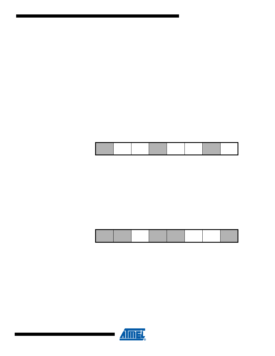
Bit
7
6
5
4
3
2
1
0
ADC7D
ADC6D
ACMPN1D
AMP2ND
ADC5D
ACMPN0D
ADC4D
ADC3D
ACMPN2D
ADC2D
ACMP2D
ADC1D
ADC0D
ACMPN3D
DIDR0
Read/Write
R/W
R/W
R/W
R/W
R/W
R/W
R/W
R/W
Initial Value
0
0
0
0
0
0
0
0
Bit
7
6
5
4
3
2
1
0
-
AMP2PD
ACMP0D
AMP0PD
AMP0ND
ADC10D
ACMP1D
ADC9D
AMP1PD
ACMP3D
ADC8D
AMP1ND
DIDR1
Read/Write
-
-
R/W
R/W
R/W
R/W
R/W
R/W
Initial Value
0
0
0
0
0
0
0
0