4 adc result data registers - adch and adcl – Rainbow Electronics ATmega64C1 User Manual
Page 245
245
7647A–AVR–02/08
ATmega32/64/M1/C1
• Bit 6 – ISRCEN: Current Source Enable
Set this bit to source a 100µA current to the AREF pin.
Clear this bit to use AREF pin as Analog Reference pin.
• Bit 5 – AREFEN: Analog Reference pin Enable
Set this bit to connect the internal AREF circuit to the AREF pin.
Clear this bit to disconnect the internal AREF circuit from the AREF pin.
• Bit 4 – Res: Reserved Bit
This bit is unused bit in the ATmega32/64/M1/C1, and will always read as zero.
• Bit 3, 2, 1, 0– ADTS3:ADTS0: ADC Auto Trigger Source Selection Bits
These bits are only necessary in case the ADC works in auto trigger mode. It means if ADATE
bit in ADCSRA register is set.
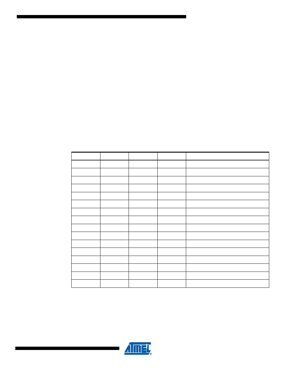
In accordance with the Table 18-7, these 3 bits select the interrupt event which will generate the
trigger of the start of conversion. The start of conversion will be generated by the rising edge of
the selected interrupt flag whether the interrupt is enabled or not. In case of trig on PSCnASY
event, there is no flag. So in this case a conversion will start each time the trig event appears
and the previous conversion is completed..
18.9.4
ADC Result Data Registers – ADCH and ADCL
When an ADC conversion is complete, the conversion results are stored in these two result data
registers.
When the ADCL register is read, the two ADC result data registers can’t be updated until the
ADCH register has also been read.
Consequently, in 10-bit configuration, the ADCL register must be read first before the ADCH.
Table 18-7.
ADC Auto Trigger Source Selection
ADTS3
ADTS2
ADTS1
ADTS0
Description
0
0
0
0
Free Running Mode
0
0
0
1
External Interrupt Request 0
0
0
1
0
Timer/Counter0 Compare Match
0
0
1
1
Timer/Counter0 Overflow
0
1
0
0
Timer/Counter1 Compare Match B
0
1
0
1
Timer/Counter1 Overflow
0
1
1
0
Timer/Counter1 Capture Event
0
1
1
1
PSC Module 0 Synchronization Signal
1
0
0
0
PSC Module 1 Synchronization Signal
1
0
0
1
PSC Module 2 Synchronization Signal
1
0
1
0
Analog comparator 0
1
0
1
1
Analog comparator 1
1
1
0
0
Analog comparator 2
1
1
0
1
Analog comparator 3
1
1
1
0
Reserved
1
1
1
1
Reserved