4 analog comparator register description, 1 analog comparator 0 control register - ac0con – Rainbow Electronics ATmega64C1 User Manual
Page 260
260
7647A–AVR–02/08
ATmega32/64/M1/C1
20.4
Analog Comparator Register Description
Each analog comparator has its own control register.
A dedicated register has been designed to consign the outputs and the flags of the 4 analog
comparators.
20.4.1
Analog Comparator 0 Control Register – AC0CON
• Bit 7– AC0EN: Analog Comparator 0 Enable Bit
Set this bit to enable the analog comparator 0.
Clear this bit to disable the analog comparator 0.
• Bit 6– AC0IE: Analog Comparator 0 Interrupt Enable bit
Set this bit to enable the analog comparator 0 interrupt.
Clear this bit to disable the analog comparator 0 interrupt.
• Bit 5, 4– AC0IS1, AC0IS0: Analog Comparator 0 Interrupt Select bit
These 2 bits determine the sensitivity of the interrupt trigger.
The different setting are shown in
• Bit 3 – ACCKSEL: Analog Comparator Clock Select
Set this bit to use the PLL output as comparator clock.
Clear this bit to use the CLK
IO
as comparator clock.
• Bit 2, 1, 0– AC0M2, AC0M1, AC0M0: Analog Comparator 0 Multiplexer register
These 3 bits determine the input of the negative input of the analog comparator.
The different setting are shown in
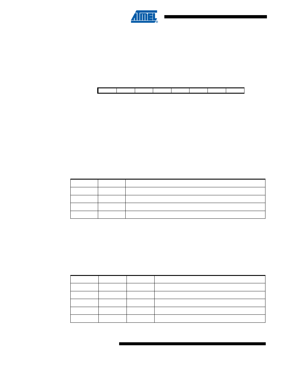
Bit
7
6
5
4
3
2
1
0
AC0EN
AC0IE
AC0IS1
AC0IS0
ACCKSEL
AC0M2
AC0M1
AC0M0
AC0CON
Read/Write
R/W
R/W
R/W
R/W
R/W
R/W
R/W
R/W
Initial Value
0
0
0
0
0
0
0
0
Table 20-1.
Interrupt sensitivity selection
AC0IS1
AC0IS0
Description
0
0
Comparator Interrupt on output toggle
0
1
Reserved
1
0
Comparator interrupt on output falling edge
1
1
Comparator interrupt on output rising edge
Table 20-2.
Analog Comparator 0 negative input selection
AC0M2
AC0M1
AC0M0
Description
0
0
0
“Vref”/6.40
0
0
1
“Vref”/3.20
0
1
0
“Vref”/2.13
0
1
1
“Vref”/1.60
1
0
0
Bandgap (1.1V)