1 user calibration, 2 manufacturing calibration, 9 adc register description – Rainbow Electronics ATmega64C1 User Manual
Page 241: 1 adc multiplexer register - admux
241
7647A–AVR–02/08
ATmega32/64/M1/C1
The measured voltage has a linear relationship to the temperature as described in
. The voltage sensitivity is approximately 1 mV/
°
C and the accuracy of the temperature
measurement is +/- 10°C after bandgap calibration.
The values described in
are typical values. However, due to the process
variation the temperature sensor output voltage varies from one chip to another. To be capable
of achieving more accurate results, the temperature measurement can be calibrated in the appli-
cation software.
18.8.1
User Calibration
The software calibration requires that a calibration value is measured and stored in a register or
EEPROM for each chip. The software calibration can be done utilizing the formula:
T = { [ (ADCH << 8) | ADCL ] - T
OS
} / k
where ADCH & ADCL are the ADC data registers, k is a fixed coefficient and T
OS
is the temper-
ature sensor offset value determined and stored into EEPROM.
18.8.2
Manufacturing Calibration
One can also use the calibration values available in the signature row
ture Row from Software” on page 283.
The calibration values are determined from values measured during test at room temperature
which is approximatively +25°C and during test at hot temperature which is approximatively
+125°C.
The temperature in Celsius degrees can be calculated utilizing the formula:
T = { [ (ADCH << 8) | ADCL ] *TSGAIN } +TSOFFSET-273
Where:
a.
ADCH & ADCL are the ADC data registers,
b.
TSGAIN is the temperature sensor gain (constant 1, or unsigned fixed point num-
ber, 0x80 = decimal 1.0)
c.
TSOFFSET is the temperature sensor offset correction term (2. complement
signed byte)
18.9
ADC Register Description
The ADC of the ATmega32/64/M1/C1 is controlled through 3 different registers. The ADCSRA
and The ADCSRB registers which are the ADC Control and Status registers, and the ADMUX
which allows to select the Vref source and the channel to be converted.
The conversion result is stored on ADCH and ADCL register which contain respectively the most
significant bits and the less significant bits.
18.9.1
ADC Multiplexer Register – ADMUX
Table 18-3.
Temperature vs. Sensor Output Voltage (Typical Case)
Temperature /
°C
-40
°C
+25
°C
+125
°C
Voltage / mV
600 mV
762 mv
1012 mV
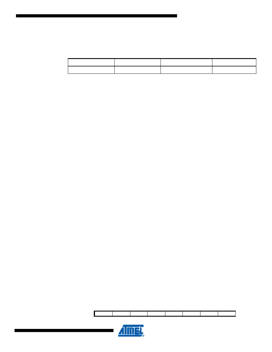
Bit
7
6
5
4
3
2
1
0
REFS1
REFS0
ADLAR
MUX4
MUX3
MUX2
MUX1
MUX0
ADMUX