Rainbow Electronics W90N745CDG User Manual
Page 78
W90N745CD/W90N745CDG
Publication Release Date: September 22, 2006
-
73
-
Revision
A2
Continued.
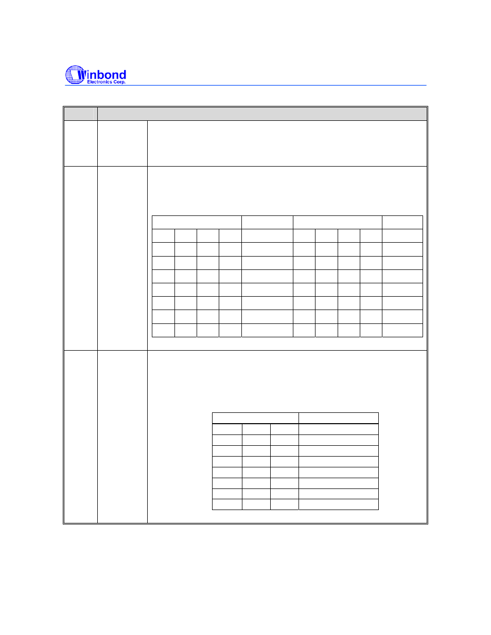
BITS
DESCRIPTION
[15] ADRS
Address bus alignment for external I/O bank 0~3
When ADRS is set, external address (A20~A0) bus is alignment to byte
address format, that is, A0 is internal AHB address bus HADDR[0] and A1 is
AHB bus HADDR[1] and so forth. And it ignores DBWD [1:0] setting.
[14:11] tACC
Access cycles of external I/O bank 0~3
This parameter means nWE, nWBE and nOE active time clock. Detail timing
diagram please refer to Figure 6.3.6 and 6.3.7
tACC[14:11] MCLK tACC[14:11]
MCLK
0 0 0 0 Reversed 1 0 0 0
9
0 0 0 1
1
1 0 0 1 11
0 0 1 0
2
1 0 1 0 13
0 0 1 1
3
1 0 1 1 15
0 1 0 0
4
1 1 0 0 17
0 1 0 1
5
1 1 0 1 19
0 1 1 0
6
1 1 1 0 21
0 1 1 1
7
1 1 1 1 23
[10:8] tCOH
Chip selection hold time of external I/O bank 0~3
This parameters control nWBE and nOE hold time. Detail timing diagram
please refer to Figure 6.3.6 and 6.3.7
tCOH [10:8]
MCLK
0 0 0
0
0 0 1
1
0 1 0
2
0 1 1
3
1 0 0
4
1 0 1
5
1 1 0
6
1 1 1
7