Data transfer – Rainbow Electronics W90N745CDG User Manual
Page 345

W90N745CD/W90N745CDG
Publication Release Date: September 22, 2006
-
341
-
Revision
A2
Data Transfer
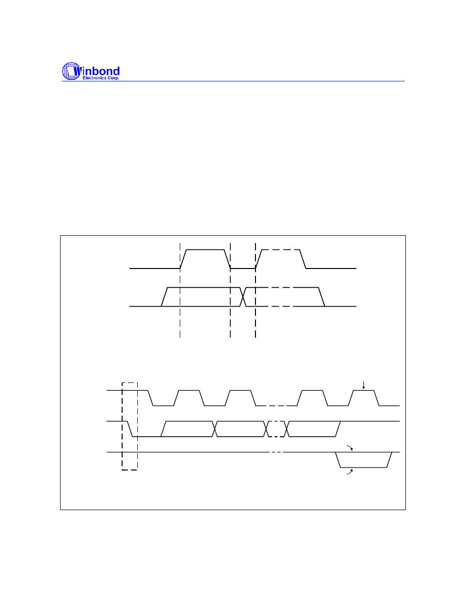
Once successful slave addressing has been achieved, the data transfer can proceed on a byte-by-
byte basis in the direction specified by the RW bit sent by the master. Each transferred byte is
followed by an acknowledge bit on the 9th SCL clock cycle. If the slave signals a Not Acknowledge
(NACK), the master can generate a STOP signal to abort the data transfer or generate a Repeated
START signal and start a new transfer cycle.
If the master, as the receiving device, does Not Acknowledge (NACK) the slave, the slave releases
the SDA line for the master to generate a STOP or Repeated START signal.
To write data to a slave, store the data to be transmitted in the Transmit Register (TxR) and set the
WRITE bit. To read data from a slave, set the READ bit. During a transfer the core set the I
2
C_TIP
flag, indicating that a Transfer is In Progress. When the transfer is done the I
2
C_TIP flag is cleared,
the IF flag set if enabled, then an interrupt generated. The Receive Register (RxR) contains valid data
after the IF flag has been set. The software may issue a new write or read command when the
I
2
C_TIP flag is cleared.
data line
stable;
data valid
change
of data
allowed
SCL
SDA
Bit transfer on the I
2
C-bus
1
2
8
9
SCL FROM
MASTER
DATA OUTPUT BY
TRANSMITTER
DATA OUTPUT BY
RECEIVER
S
START
condition
clock pulse for
acknowledgement
not acknowledge
acknowledge
Acknowledge on the I
2
C-bus
