Rainbow Electronics W90N745CDG User Manual
Page 72

W90N745CD/W90N745CDG
Publication Release Date: September 22, 2006
-
67
-
Revision
A2
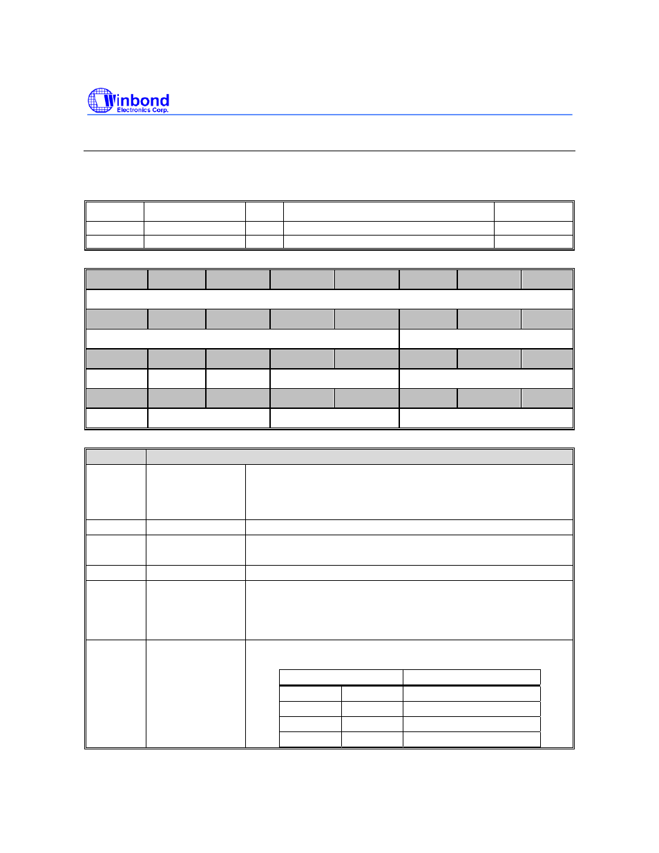
Configuration Registers(SDCONF0/1)
The configuration registers enable software to set a number of operating parameters for the SDRAM
controller. There are two configuration registers SDCONF0、SDCONF1 for SDRAM bank 0、bank 1
respectively. Each bank can have a different configuration.
REGISTER ADDRESS R/W
DESCRIPTION
RESET
VALUE
SDCONF0
0xFFF0_1008
R/W SDRAM bank 0 configuration register
0x0000_0800
SDCONF1
0xFFF0_100C
R/W SDRAM bank 1 configuration register
0x0000_0800
31
30
29
28
27
26
25
24
BASADDR
23
22
21
20
19
18
17
16
BASADDR
RESERVED
15
14
13
12
11
10
9
8
MRSET
RESERVED
AUTOPR
LATENCY
RESERVED
7
6
5
4
3
2
1
0
COMPBK DBWD
COLUMN
SIZE
BITS
DESCRIPTION
[31:19] BASADDR
Base address pointer of SDRAM bank 0/1
The start address is calculated as SDRAM bank 0/1 base pointer
<< 18. The SDRAM base address pointer together with the “SIZE”
bits constitutes the whole address range of each SDRAM bank.
[18:16] RESERVED
-
[15] MRSET
SDRAM Mode register set command for SDRAM bank 0/1
This bit set will issue a mode register set command to SDRAM.
[14] RESERVED
-
[13] AUTOPR
Auto pre-charge mode of SDRAM for SDRAM bank 0/1
Enable the auto pre-charge function of external SDRAM bank 0/1
0 = Auto pre-charge
1 = No auto pre-charge
[12:11] LATENCY
The CAS Latency of SDRAM bank 0/1
Defines the CAS latency of external SDRAM bank 0/1
LATENCY [12:11]
MCLK
0 0
1
0 1
2
1 0
3
1 1 REVERSED
