Functional description, 1 arm7tdmi cpu core – Rainbow Electronics W90N745CDG User Manual
Page 29
W90N745CD/W90N745CDG
- 24 -
6. FUNCTIONAL
DESCRIPTION
6.1 ARM7TDMI CPU CORE
The ARM7TDMI CPU core is a member of the Advanced RISC Machines (ARM) family of general-
purpose 32-bit microprocessors, which offer high performance for very low power consumption. The
architecture is based on Reduced Instruction Set Computer (RISC) principles, and the instruction set and
related decode mechanism are much simpler than those of micro-programmed Complex Instruction Set
Computers. Pipelining is employed so that all parts of the processing and memory systems can operate
continuously. The high instruction throughput and impressive real-time interrupt response are the major
benefits.
The ARM7TDMI CPU core has two instruction sets:
(1) The standard 32-bit ARM set
(2) A 16-bit THUMB set
The THUMB set’s 16-bit instruction length allows it to approach twice the density of standard ARM core
while retaining most of the ARM’s performance advantage over a traditional 16-bit processor using 16-bit
registers. THUMB instructions operate with the standard ARM register configuration, allowing excellent
interoperability between ARM and THUMB states. Each 16-bit THUMB instruction has a corresponding
32-bit ARM instruction with the same effect on the processor model.
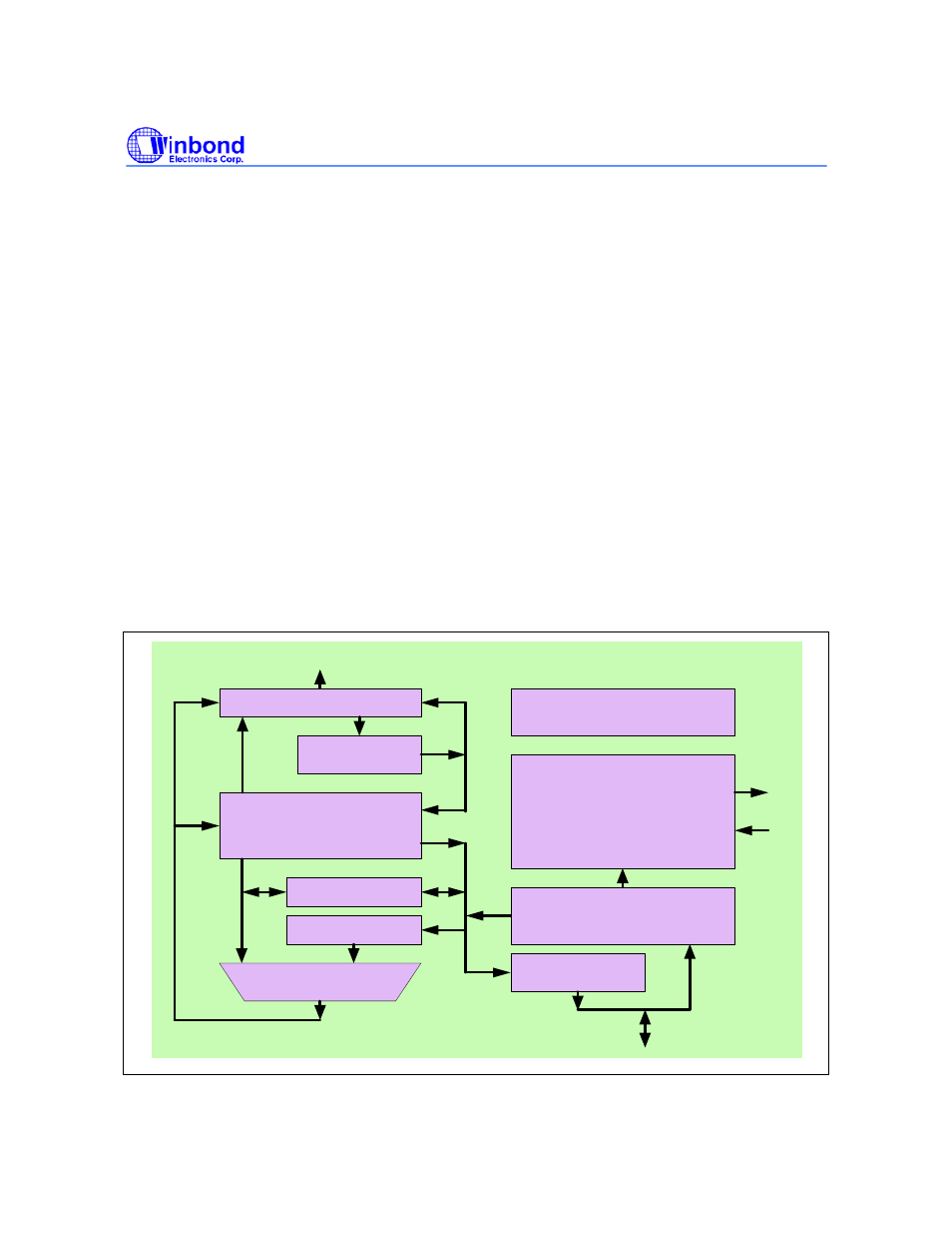
ARM7TDMI CPU core has 31 x 32-bit registers. At any one time, 16 sets are visible; the other registers
are used to speed up exception processing. All the register specified in ARM instructions can address
any of the 16 registers. The CPU also supports 5 types of exception, such as two levels of interrupt,
memory aborts, attempted execution of an undefined instruction and software interrupts.
Address Register
Address
Incrementer
Barrel Shifter
Register Bank
(31 x 32-bit registers)
(6 status registers)
32 x8 Multiplier
32-bit ALU
Writer Data
Register
Instruction Pipeline
Read Data Register
Thumb Instruction Decoder
Instruction Decoder
Control Logic
Scan Control
B Bu
s
A Bu
s
ALU
B
u
s
PC
Bu
s
Inc
re
m
enter
B
u
s
A[31:0]
D[31:0]
Figure 6.1.1 ARM7TDMI CPU Core Block Diagram