Rainbow Electronics W90N745CDG User Manual
Page 33

W90N745CD/W90N745CDG
- 28 -
6.2.3 Address Bus Generation
The W90N745 address bus generation is depended on the required data bus width of each memory
bank. The data bus width is determined by DBWD bits in each bank’s control register.
The maximum accessible memory size of each external IO bank is 4M bytes.
Table 6.2.2 Address Bus Generation Guidelines
DATA BUS
EXTERNAL ADDRESS PINS
WIDTH A
[20:0]
MAXIMUM ACCESSIBLE MEMORY SIZE
8-bit
A20 – A0
(Internal)
2M bytes
16-bit
A21 – A1
(Internal)
2M half-words
6.2.4 Data Bus Connection with External Memory
6.2.4.1. Memory formats
The W90N745 can be configured as big endian or little endian mode by pull up or down the external data
bus D14 pin. If D14 is pull up, then it is a little endian mode, otherwise, it is a big endian mode.
Little endian
In little endian format, the lowest addressed byte in a word is considered the least significant byte of the
word and the highest addressed byte is the most significant. So the byte at address 0 of the memory
system connects to data lines 7 through 0.
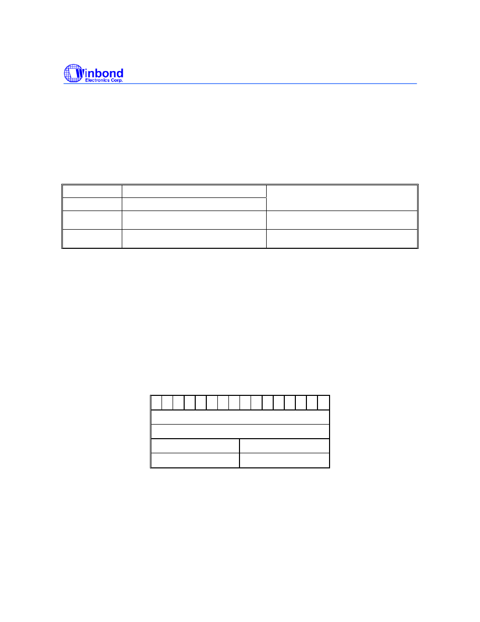
For a word aligned address A, Figure 6.2.2 shows how the half-word at addresses A and A+2, and the
bytes at addresses A, A+1, A+2, and A+3 map on to each other when D14 pin is High.
15 14 13 12 11 10 9
8
7
6
5
4
3
2
1
0
Half-word at address A
Half-word at address A+2
Byte at address A+1
Byte at address A
Byte at address A+3
Byte at address A+2
Figure 6.2.2 Little endian addresses of bytes and half-words within half words
