4 lbc timing parameters, Table 7-5, Lbc timing parameters – Artesyn MVME2502 Installation and Use (April 2015) User Manual
Page 152: Programming model
Programming Model
MVME2502 Installation and Use (6806800R96E)
152
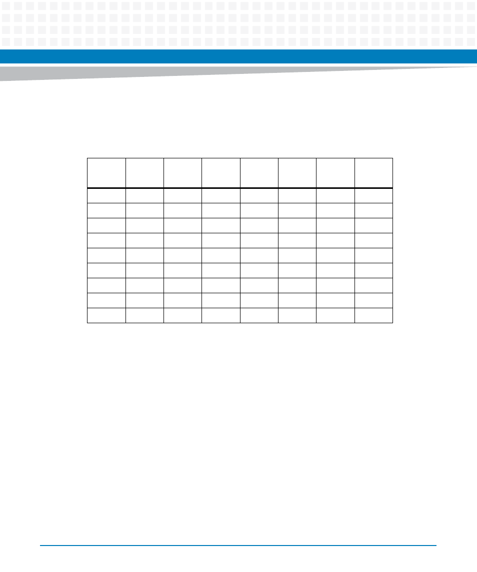
7.6.4
LBC Timing Parameters
The following table defines the timing parameters for the devices on the local bus.
Table 7-5 LBC Timing Parameters
0
1
2
3
4
5
6
MRAM
UART 0
UART 1
UART 2
UART 3
CPLD
Timers
BCTLD
0
0
0
0
0
0
0
CSNT
1
1
1
1
1
1
1
ACS
10
10
10
10
10
10
10
XACS
0
0
0
0
0
0
0
SCY
0011
0011
0011
0011
0011
0011
0011
SETA
0
0
0
0
0
0
0
TRLX
0
0
0
0
0
0
0
EHTR
0
0
0
0
0
0
0
EAD
0
0
0
0
0
0
0
Field Description
BCTLD
Buffer control disable.
0 - LBCTL is asserted upon access to the current memory bank.
CSNT
Chip Select negation time.
1 - LCSn and LWE are negated one quarter of the bus clock cycle earlier
ACS
Address to chip-select setup.
10 - LCSn is outputted one quarter bus clock cycle after the address lines.
XACS
Extra Address to chip-select setup
0 - Address to chip-select setup is determined by ORx[ACS]
SCY
Cycle length in bus clocks
0011 - bus clock cycle wait state
- MVME2502 Installation and Use (August 2014) MVME2500 Installation and Use Manual (February 2014) MVME2500 ECC Installation and Use (August 2014) MVME2500 Installation and Use (April 2015) MVME2500 Installation and Use Manual (March 2015) MVME2502 Installation and Use (April 2014) MVME2502 Installation and Use (December 2014)