Programming model, 1 overview, 2 reset configuration – Artesyn MVME2502 Installation and Use (April 2015) User Manual
Page 145: 1 overview 7.2 reset configuration, Table 7-1, Por configuration settings, Chapter 7
Chapter 7
MVME2502 Installation and Use (6806800R96E)
145
Programming Model
7.1
Overview
This chapter includes additional programming information for the MVME2502.
7.2
Reset Configuration
The MVME2502 supports the power-on reset (POR) pin sampling method for processor reset
configuration. Each option and the corresponding default setting are described in the
following table.
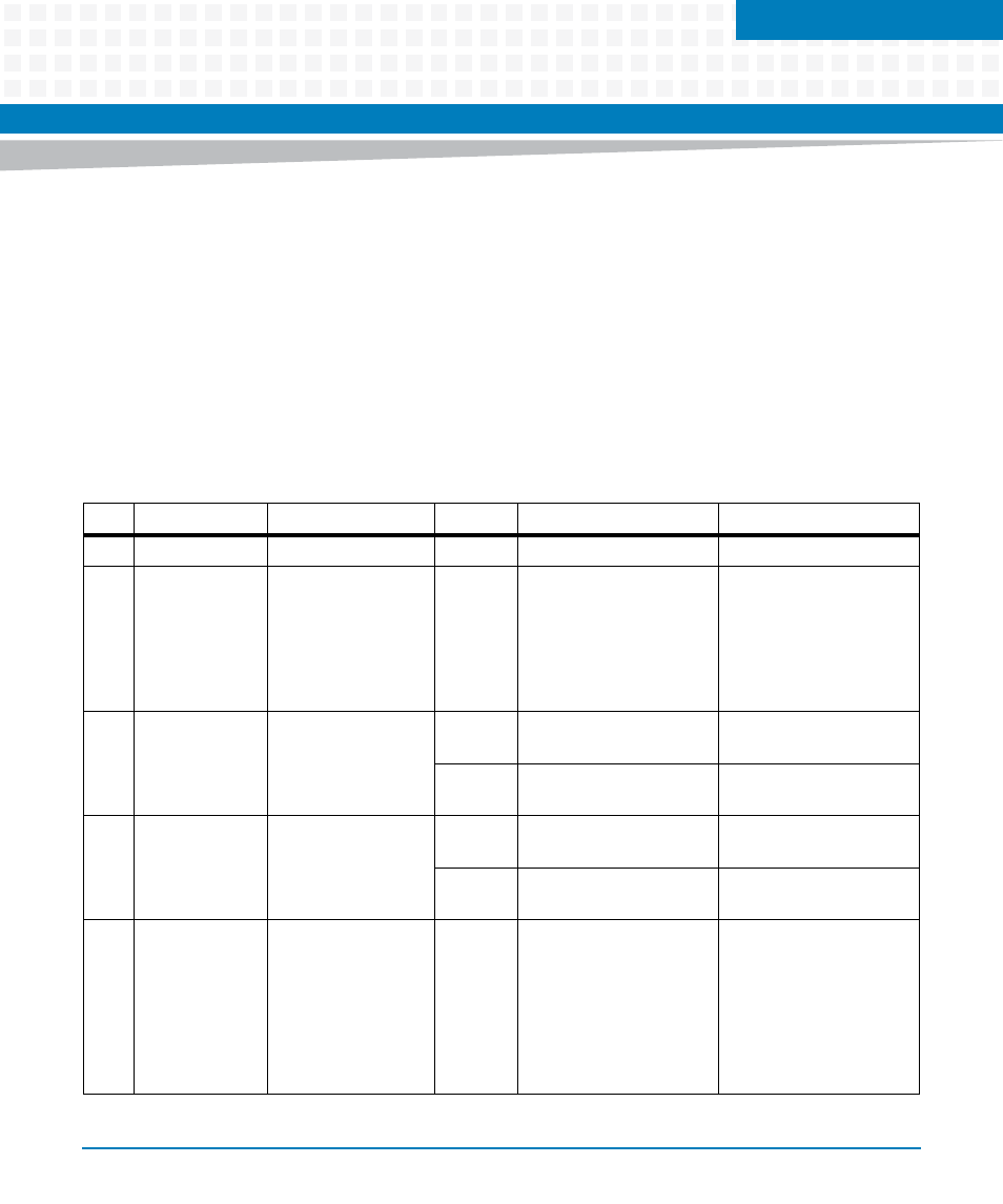
Table 7-1 POR Configuration Settings
CONFIG
CONFIG PINS
CONFIG
SELECTION
REMARKS
1
CCB Config
LA[29:31]
000
41: CCB CLOCK-400 MHz
2
DDR PLL Config
TSEC_1588_CLK_O
UT
TSEC_1588_PULSE_
OUT1
TSEC_1588_PULSE_
OUT2
001
8:1 DDR PLL-800 MHz
DDR rate is twice the
value of the DDR
controller frequency,
which is then divided by
two through the
software.
3
Core 0 PLL
LBCTL, LALE
LGPL2/LOE/LFRE
110
3:1 CORE CLOCK PLL
(1200 MHz)
For 1200 MHz board
configuration
100
2:1 CORE CLOCK PLL (800
MHz)
For 800 MHz board
configuration
4
Core 1 PLL
LWE0, UART_SOUT1
110
3:1 CORE CLOCK PLL
(1200 MHz)
For 1200 MHz board
configuration
100
2:1 CORE CLOCK PLL (800
MHz)
For 800 MHz board
configuration
5
CPU Boot
Config
LA27, LA16
10
e500 core 0 is allowed to
boot without waiting for
configuration by an
external master, while
e500 core 1 is prevented
from booting until
configured by an external
master or the other core.
- MVME2502 Installation and Use (August 2014) MVME2500 Installation and Use Manual (February 2014) MVME2500 ECC Installation and Use (August 2014) MVME2500 Installation and Use (April 2015) MVME2500 Installation and Use Manual (March 2015) MVME2502 Installation and Use (April 2014) MVME2502 Installation and Use (December 2014)