Cp3bt26 – National CP3BT26 User Manual
Page 94

www.national.com
94
CP3BT26
18.3.1
Main Control Register (MCNTRL)
The MCNTRL register controls the main functions of the
CR16 USB node. The MCNTRL register provides read/write
access from the CPU bus. Reserved bits must be written
with 0, and they return 0 when read. It is clear after reset.
USBEN
The USB Enable controls whether the USB
module is enabled. If the USB module is dis-
abled, the 48 MHz clock within the USB node
is stopped, all USB registers are initialized to
their reset state, and the USB transceiver forc-
es SE0 on the bus to prevent the hub from de-
tected the USB node. The USBEN bit is clear
after reset.
0 – The USB module is disabled.
1 – The USB module is enabled.
EPC0
FF FDC0h
Endpoint Control 0
Register
EPC1
FF FDD0h
Endpoint Control 1
Register
EPC2
FF FDD8h
Endpoint Control 2
Register
EPC3
FF FDE0h
Endpoint Control 3
Register
EPC4
FF FDDE8h
Endpoint Control 4
Register
EPC5
FF FDF0h
Endpoint Control 5
Register
EPC6
FF FDF8h
Endpoint Control 6
Register
TXS0
FF FDC4h
Transmit Status 0
Register
TXS1
FF FDD4h
Transmit Status 1
Register
TXS2
FF FDE4h
Transmit Status 2
Register
TXS3
FF FDF4h
Transmit Status 3
Register
TXC0
FF FDC6h
Transmit Command 0
Register
TXC1
FF FDD6
Transmit Command 1
Register
TXC2
FF FDE6h
Transmit Command 2
Register
TXC3
FF FDF6h
Transmit Command 3
Register
TXD0
FF FDC2h
Transmit Data 0
Register
TXD1
FF FDD2h
Transmit Data 1
Register
TXD2
FF FDE2h
Transmit Data 2
Register
TXD3
FF FDF2h
Transmit Data 3
Register
RXS0
FF FDCCh
Receive Status 0
Register
RXS1
FF FDDCh
Receive Status 1
Register
RXS2
FF FDECh
Receive Status 2
Register
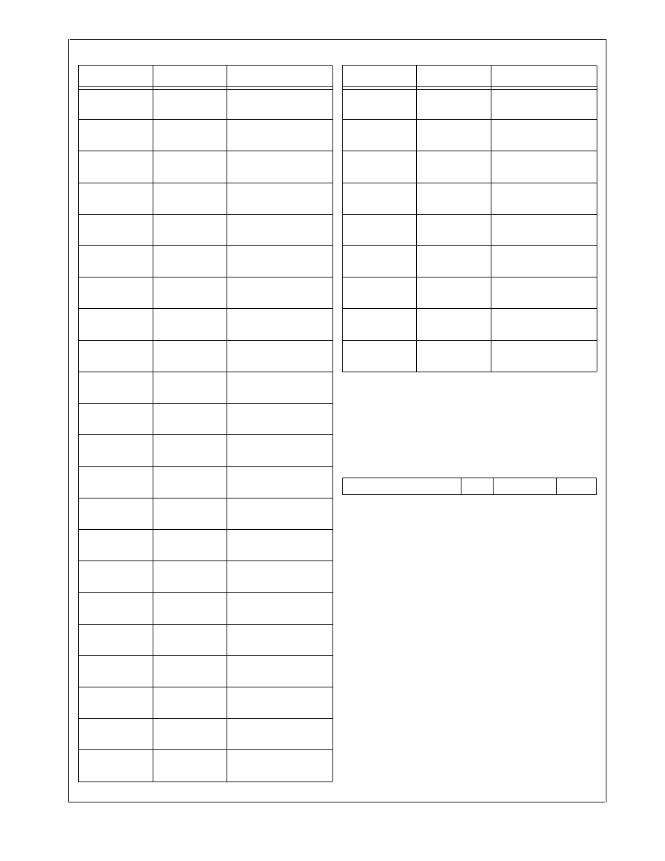
Table 40
USB Controller Registers
Name
Address
Description
RXS3
FF FDFCh
Receive Status 3
Register
RXC0
FF FDCEh
Receive Command 0
Register
RXC1
FF FDDEh
Receive Command 1
Register
RXC2
FF FDEEh
Receive Command 2
Register
RXC3
FF FDFEh
Receive Command 3
Register
RXD0
FF FDCAh
Receive Data 0
Register
RXD1
FF FDDAh
Receive Data 2
Register
RXD2
FF FDEAh
Receive Data 2
Register
RXD3
FF FDFAh
Receive Data 3
Register
7
4
3
2
1
0
Reserved
NAT
Reserved
USBEN
Table 40
USB Controller Registers
Name
Address
Description
