Figure 18, Figure 19 sho, Cp3 bt26 – National CP3BT26 User Manual
Page 75

75
www.national.com
CP3
BT26
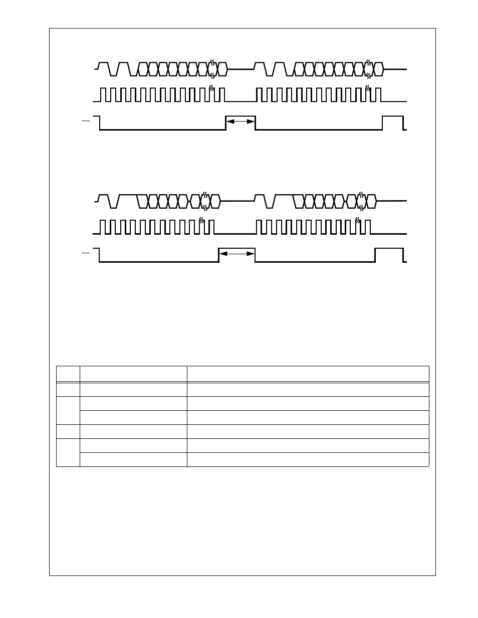
Figure 18.
32-Bit Write Timing
Figure 19.
32-Bit Read Timing
An example of a 32-bit write is shown in Table 31. In this ex-
ample, the 32-bit value FFFF DC04h is written to register
address 0Ah. In cycle 1, the high word (FFFFh) is written. In
the first part of cycle 2, the CP3BT26 drives the header, R/
W bit, and register address for a read cycle. In the second
part of cycle 2, the LMX5252 drives the counter value. The
counter value is 0, which indicates one word has been writ-
ten. In cycle 3, the low word (DC04h) is written. In the first
part of cycle 4, the CP3BT26 drives the header, R/W bit,
and register address for a read cycle. In the second part of
cycle 4, the LMX5252 drives the counter value. The counter
value is 1, which indicates two words have been written.
SLE
SCLK
SDAT
DS322
D16
D30
A0
A1
A2
A3
A4
W
H0
H1
H2
D31
D0
D14
A0
A1
A2
A3
A4
W
H0
H1
H2
D15
>500 ns
SLE
SCLK
SDAT
DS323
D16
D31
A0
A1
A2
A3
A4
R
H0
H1
H2
D0
D15
A0
A1
A2
A3
A4
R
H0
H1
H2
>500 ns
Table 31
Example of 32-Bit Write with Interleaved Reads
Cycle
Serial Data on SDAT
Description
1
101 0 01010 1111111111111111
Write cycle driven by CP3BT26. Data is FFFFh. Address is 0Ah.
2
101 1 01010
First part of read cycle driven by CP3BT26. Address is 0Ah.
0000000000000000
Second part of read cycle driven by LMX5252. Counter value is 0.
3
101 0 01010 1101110000000100
Write cycle driven by CP3BT26. Data is DC04h. Address is 0Ah.
4
101 1 01010
First part of read cycle driven by CP3BT26. Address is 0Ah.
0000000000000001
Second part of read cycle driven by LMX5252. Counter value is 1.
