Cp3bt26 – National CP3BT26 User Manual
Page 82

www.national.com
82
CP3BT26
16.2.2
Measuring Pen Force
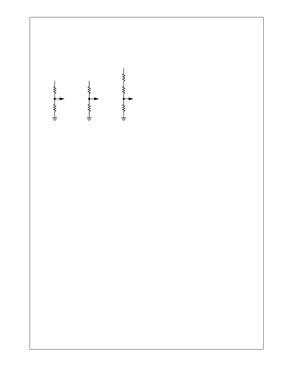
Figure 27 shows equivalent circuits for the driver modes
used to measure the X, Y, and Z coordinates, in which Z rep-
resents pen force. In this discussion, the ohmic resistance
of the drivers is neglected (see Section 16.2.3), and series
resistance between the node of interest and the ADC is ig-
nored because it has no significant effect.
Figure 27.
Touchscreen Driver Modes
In the following examples, the ADC is assumed to operate
in single-ended mode to produce conversion values be-
tween 0 and 2047, however the same principles could be
extended to differential mode to recover the full range of the
ADC.
In Sample X mode, the X plate is driven between VCC and
ground, so that a value measured at node A on the TSY+ or
TSY- inputs is the center tap of a resistor-divider network.
The end-to-end resistance RXP of the X plate is:
The value measured at node A is proportional to the ratio
between the resistance to ground and the resistance of the
X plate:
Solving for RX2, the resistance is:
Similarly, in Sample Y mode the value measured at node B
on the TSX+ or TSX- inputs is proportional to the ratio be-
tween the resistance to ground and the resistance RYP of
the Y plate:
Because end-to-end resistance RYP of the Y plate is:
The previous equation can be rewritten as:
Solving for RY1, the resistance is:
Now that the resistance values RX2 and RY1 are known, it
is possible to calculate the value of the plate-to-plate con-
tact resistance, RZ, given the value measured at node C on
the TSX+ input in Sample Z mode. Node C is a tap in a re-
sistor-divider network composed of three resistors, such
that:
Solving for RZ, the resistance is:
The resistance RZ is proportional to the force of pen con-
tact.
16.2.3
Compensation for Driver Resistance
Plate resistances between opposite electrodes range from
100 ohms to 1k ohm. Because of the 6-ohm driver resis-
tance, some significant voltage drop will be experienced be-
tween, for example, TSX- and AGND. A 200-ohm plate will
drop:
With a 2.5V supply, this is 70 mV. A 12-bit ADC has 4096
possible values, so each value covers a range of 610 µV at
2.5V. A voltage drop of 70 mV across each of the low-ohmic
drivers reduces the number of available ADC values by:
This effective loss of resolution can be handled in a number
of ways.
1. The voltages on, for example, TSY+ and TSY- can be
sampled before sampling TSX+ and TSX-. Then, scal-
ing can be applied in software to convert the samples
to the full (4096-bit) range. This technique will not re-
cover any resolution, however it is worthy of some con-
sideration because touchscreen data is typically
passed to two applications:
Signature Analysis—only the raw data is required. No
absolute positioning is necessary.
Screen Overlay—for example, for cursor positioning.
In this application, a scaling or calibration is performed
to correctly overlay the touchscreen coordinates onto
the display. Because of this calibration, it is not even
necessary to sample TSY+ and TSY-.
2. The ADC has a positive voltage reference input which
can be internally connected to the TSY+ terminal. This
means that the number of available ADC values is in-
creased to:
Software scaling could be applied to this value if re-
quired (as with technique 1, above), but no additional
resolution is achieved.
DS188
VCC
RX1
RX2
A
Sample X
TOUCH_CFG = 001
VCC
RY1
RY2
B
Sample Y
TOUCH_CFG = 010
RZ
RX2
C
VCC
RY1
Sample Z
TOUCH_CFG = 100
RXP
RX1
RX2
+
=
A
2047
-------------
RX2
RXP
-------------
=
RX2
RXP
A
2047
-------------
×
=
B
2047
-------------
RY2
RYP
-------------
=
RYP
RY1
RY2
+
=
B
2047
-------------
RYP
RY1
–
RYP
-------------------------------
=
RY1
RYP
1
B
2047
-------------
–
×
=
C
2047
-------------
RX2
RY1
RZ
RX2
+
+
----------------------------------------------
=
RZ
RX2
2047
C
–
C
-----------------------
×
RY1
–
=
6
200
6
6
+
+
-----------------------------
AVCC
AGND
–
(
)
×
70 mV
2
×
610 uV
--------------------------
230
=
4096
70 mV
610 uV
--------------------
–
3981
=
