Cp3bt26 – National CP3BT26 User Manual
Page 144

www.national.com
144
CP3BT26
20.2.2
Synchronous Mode
In synchronous mode, the receive and transmit paths of the
audio interface use the same shift clock and frame sync sig-
nal. The bit shift clock and frame sync signal for both paths
are derived from the same set of clock prescalers.
20.2.3
Normal Mode
In normal mode, each rising edge on the frame sync signal
marks the beginning of a new frame and also the beginning
of a new slot. A slot does not necessarily occupy the entire
frame. (A frame can be longer than the data word transmit-
ted after the frame sync pulse.) Typically, a codec starts
transmitting a fixed length data word (e.g. 8-bit log PCM da-
ta) with the frame sync signal, then the codec’s transmit pin
returns to the high-impedance state for the remainder of the
frame.
The Audio Receive Shift Register (ARSR) de-serializes re-
ceived on the SRD pin (serial receiver data). Only the data
sampled after the frame sync signal are treated as valid. If
the interface is interrupt-driven, valid data bits are trans-
ferred from the ARSR to the receive FIFO. If the interface is
configured for DMA, the data is transferred to the receive
DMA register 0 (ARDR0).
The serial transmit data (STD) pin is only an active output
while data is shifted out. After the defined number of data
bits have been shifted out, the STD pin returns to the high-
impedance state.
For operation in normal mode, the Slot Count Select bits
(SCS[1:0]) in the Global Configuration register (AGCR)
must be loaded with 00b (one slot per frame). In addition,
the Slot Assignment bits for receive and transmit must be
programmed to select slot 0.
If the interface is configured for DMA, the DMA slot assign-
ment bits must also be programmed to select slot 0. In this
case, the audio data is transferred to or from the receive or
transmit DMA register 0 (ARDR0/ATDR0).
Figure 65 shows the frame timing while operating in normal
mode with a long frame sync interval.
Figure 65.
Normal Mode Frame
IRQ Support
If the receiver interface is configured for interrupt-driven I/O
(RXDSA0 = 0), all received data are loaded into the receive
FIFO. An IRQ is asserted as soon as the number of data
bytes or words in the receive FIFO is greater than a pro-
grammable warning limit.
If the transmitter interface is configured for interrupt-driven
I/O (TXDSA0 = 0), all data to be transmitted is read from the
transmit FIFO. An IRQ is asserted as soon as the number
data bytes or words available in the transmit FIFO is equal
or less than a programmable warning limit.
DMA Support
If the receiver interface is configured for DMA (RXDSA0 =
1), received data is transferred from the ARSR into the DMA
receive buffer 0 (ARDR0). A DMA request is asserted when
the ARDR0 register is full. If the transmitter interface is con-
figured for DMA (TXDSA0 = 1), data to be transmitted are
read from the DMA transmit buffer 0 (ATDR0). A DMA re-
quest is asserted to the DMA controller when the ATDR0
register is empty.
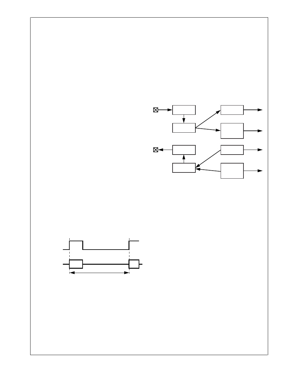
Figure 66 shows the data flow for IRQ and DMA mode in
normal Mode.
Figure 66.
IRQ/DMA Support in Normal Mode
Network Mode
In network mode, each frame is composed of multiple slots.
Each slot may transfer 8 or 16 bits. All of the slots in a frame
must have the same length. In network mode, the sync sig-
nal marks the beginning of a new frame. Only frames with
up to four slots are supported by this audio interface.
More than two devices can communicate within a network
using the same clock and data lines. The devices connected
to the same bus use a time-multiplexed approach to share
access to the bus. Each device has certain slots assigned
to it, in which only that device is allowed to transfer data.
One master device provides the bit clock and the frame sync
signal(s). On all other (slave) devices, the bit clock and
frame sync pins are inputs.
Up to four slots can be assigned to the interface, as it sup-
ports up to four slots per frame. Any other slots within the
frame are reserved for other devices.
The transmitter only drives data on the STD pin during slots
which have been assigned to this interface. During all other
slots, the STD output is in high-impedance mode, and data
can be driven by other devices. The assignment of slots to
the transmitter is specified by the Transmit Slot Assignment
bits (TXSA) in the ATCR register. It can also be specified
whether the data to be transmitted is transferred from the
transmit FIFO or the corresponding DMA transmit register.
There is one DMA transmit register (ATDRn) for each of the
maximum four data slots. Each slot can be configured inde-
pendently.
Long Frame Sync
(SFS/SRFS)
Shift Data
(STD/SRD)
Data
High-impedance
Frame
Data
DS053
DMA Slot
Assignment
TXDSA = 1
TXDSA = 0
ARSR
SRD
RX
FIFO
ARDR 0
DMA
Request 1
IRQ
DMA Slot
Assignment
RXDSA = 1
RXDSA = 0
ATSR
STD
TX
FIFO
ATDR 0
DMA
Request 0
IRQ
DS054
