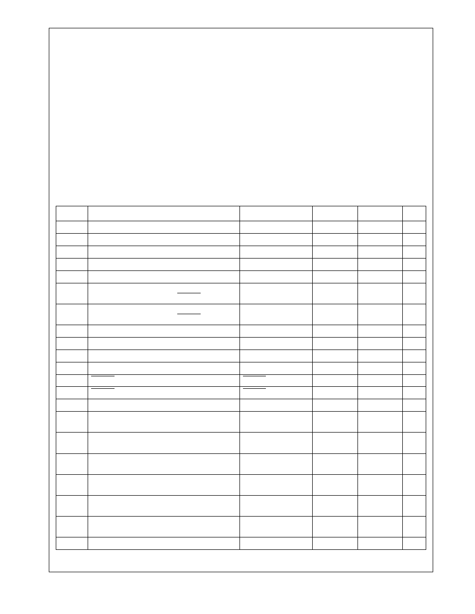
0 electrical characteristics, 1 absolute maximum ratings, Electrical characteristics – National CP3BT26 User Manual
Page 243: Absolute maximum ratings, Dc electrical characteristic, Cp3 bt26

243
www.national.com
CP3
BT26
30.0 Electrical Characteristics
30.1
ABSOLUTE MAXIMUM RATINGS
If Military/Aerospace specified devices are required, please
contact the National Semiconductor Sales Office/Distribu-
tors for availability and specifications.
Note: Absolute maximum ratings indicate limits beyond
which damage to the device may occur. DC and AC electri-
cal specifications are not ensured when operating the de-
vice at absolute maximum ratings. * The latch-up tolerance
on Access Bus pins 14 and 15 exceeds 150mA.
30.2
DC ELECTRICAL CHARACTERISTICS
(Temperature: -40°C
≤ T
A
≤ +85°C)
Supply voltage (VCC)
TBD
All input and output voltages with re-
spect to GND*
-0.5V to
IOVCC + 0.5V
ESD protection level
2 kV
(Human Body
Model)
Allowable sink/source current per
signal pin
±10 mA
Total current into IOVCC pins
200 mA
Total current into VCC pins (source)
200 mA
Total current out of GND pins (sink)
200 mA
Latch-up immunity
±200 mA
Storage temperature range
-65°C to +150°C
Symbol
Parameter
Conditions
Min
Max
Units
Vcc
Digital Logic Supply Voltage
2.25
2.75
V
IOVcc
I/O Supply Voltage
2.25
3.63
V
AVcc
Analog PLL Supply Voltage
2.25
2.75
V
ADVcc
ADC Supply Voltage
2.25
2.75
V
UVcc
USB Supply Voltage
3.0
3.63
V
V
IL
Logical 0 Input Voltage
(except X1CKI, X2CKI, and RESET)
-0.5
0.3 Vcc
V
V
IH
Logical 1 Input Voltage
(except X1CKI, X2CKI, and RESET)
0.7 IOVcc
IOVcc + 0.5
V
Vxl1
X1CKI Logical 0 Input Voltage
External X1 clock
-0.5
0.3 Vcc
V
Vxh1
X1CKI Logical 1 Input Voltage
External X1 clock
0.7 Vcc
Vcc + 0.5
V
Vxl2
X2CKI Logical 0 Input Voltage
External X2 clock
-0.5
0.6
V
Vxh2
X2CKI Logical 1 Input Voltage
External X2 clock
0.7 Vcc
Vcc + 0.5
V
Vrstl
RESET Logical 0 Input Voltage
RESET input
-0.5
0.4
V
Vrsth
RESET Logical 1 Input Voltage
RESET input
1.7
V
V
hys
Hysteresis
Loop
Width
a
0.1 IOVcc
V
I
OH
Logical 1 Output Current
V
OH
= 1.8V,
IOVcc = 2.25V
-6
mA
I
OL
Logical 0 Output Current
V
OL
= 0.45V,
IOVcc = 2.25V
6
mA
I
OLACB
SDA, SCL Logical 0 Output Current
V
OL
= 0.4V,
IOVcc = 2.25V
3
mA
I
OLTS
Touchscreen Logical 0 Output Current
(for ADC2/TSX- and ADC3/TSY-)
V
OL
= 0.15V,
ADVcc = 2.25V
18
mA
I
OHTS
Touchscreen Logical 1 Output Current
(for ADC0/TSX+ and ADC1/TSY+)
V
OH
= 2.1,
ADVcc = 2.25V
-18
mA
I
OHW
Weak Pull-up Current
V
IL
= 0V,
IOVcc = 3.63V
-20
-300
µA
I
L
High Impedance Input Leakage Current
0V
≤ Vin ≤ IOVcc -2.0
2.0
µA
