4 transceiver interface, Transceiver interface, Cp3bt26 – National CP3BT26 User Manual
Page 108

www.national.com
108
CP3BT26
18.3.36 Receive Command Register n (RXCn)
Each of the receive endpoints (2, 4, and 6) has one RXCn
register. The registers provide read/write access from the
CPU bus. Reading reserved bits returns undefined data. Af-
ter reset, it is clear.
RX_EN
The Receive Enable bit enables receiving
packets. OUT packet reception is disabled af-
ter every data packet is received, or when a
STALL handshake is returned in response to
an OUT token. The RX_EN bit must be set to
re-enable data reception. Reception of SET-
UP packets is always enabled. In the case of
back-to-back SETUP packets (for a given
endpoint) where a valid SETUP packet is re-
ceived with no other intervening non-SETUP
tokens, the Endpoint Controller discards the
new SETUP packet and returns an ACK hand-
shake. If any other reasons prevent the End-
point Controller from accepting the SETUP
packet, it must not generate a handshake.
0 – Receive disabled.
1 – Receive enabled.
IGN_SETUP The Ignore SETUP Tokens bit controls wheth-
er SETUP tokens are ignored. When this bit is
set, the endpoint ignores any SETUP tokens
directed to its configured address.
0 – Do not ignore SETUP tokens.
1 – Ignore SETUP tokens.
FLUSH
Writing 1 to the Flush bit flushes all data from
the corresponding receive FIFO, resets the
endpoint to Idle state, and clears the FIFO
read and write pointers. If the endpoint is cur-
rently using FIFO to receive data, flushing is
delayed until after the transfer is complete.
0 – Writing 0 has no effect.
1 – Writing 1 flushes the FIFOs.
RFWL
The Receive FIFO Warning Limit field speci-
fies how many more bytes can be received to
the respective FIFO before an overrun condi-
tion occurs. If the number of empty bytes re-
maining in the FIFO is equal to or less than
the selected warning limit, the RXWARN bit in
the FWEV register is set.
18.3.37 Receive Data Register n (RXD)
Each of the three Receive Endpoint FIFOs has one RXD
register. Reading the Receive Data register n returns the
data located in the receive FIFO n at the current position of
the receive read pointer. These registers provide read-only
access from the CPU bus.
RXFD
The Receive FIFO Data Byte is used to read
the receive FIFO. Software should expect to
read only the packet payload data. The PID
and CRC16 are terminated by the receive
state machine.
18.4
TRANSCEIVER INTERFACE
Separate UVCC and UGND pins are provided for the USB
transceiver, so it can be powered at the standard USB volt-
age of 3.3V while the other parts of the device run at other
voltages. The USB transceiver is powered by the system,
not the USB cable, so these pins must be connected to a
power supply and the system ground.
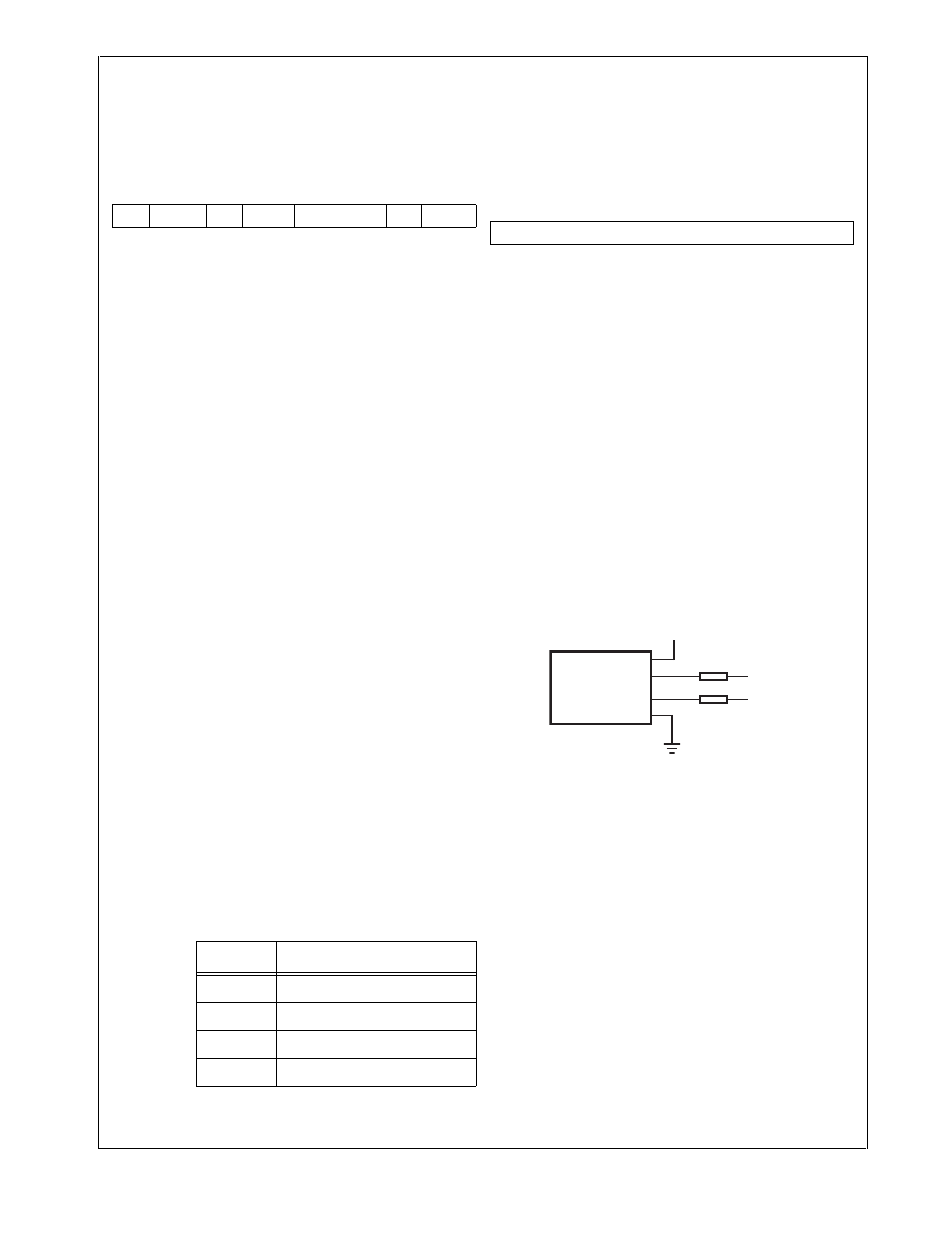
The on-chip USB transceiver does not have enough imped-
ance to meet the USB specification requirement, so exter-
nal 22-ohm resistors are required in series with the D+ and
D- pins, as shown in Figure 33.
Figure 33.
USB Transceiver Interface
7
6
5
4
3
2
1
0
Res. RFWL Res. FLUSH IGN_SETUP Res. RX_EN
Table 44
Receive FIFO Warning Limit
RFWL
Bytes Remaining in FIFO
00
RFWL disabled
01
≤ 4
10
≤ 8
11
≤ 16
7
0
RXFD
UVCC
3.3V
USB
Cable
D+
D-
UGND
22
DS231
22
CP3BT2x
