National CP3BT26 User Manual
Usb, and can interfaces, Preliminary, 0 general description

©2004 National Semiconductor Corporation
www.national.com
CP3BT26 Connectivity Pr
ocessor with
Bluetooth and Dual CAN Interfaces
PRELIMINARY
MAY 2004
CP3BT26 Reprogrammable Connectivity Processor with
Bluetooth
®
, USB, and CAN Interfaces
1.0
General Description
The CP3BT26 connectivity processor combines high perfor-
mance with the massive integration needed for embedded
Bluetooth applications. A powerful RISC core with on-chip
SRAM and Flash memory provides high computing band-
width, hardware communications peripherals provide high-
I/O bandwidth, and an external bus provides system ex-
pandability.
On-chip communications peripherals include: Bluetooth
Lower Link Controller, Universal Serial Bus (USB) 1.1 node,
CAN, Microwire/Plus, SPI, ACCESS.bus, quad UART, 12-bit
A/D converter, and Advanced Audio Interface (AAI). Addi-
tional on-chip peripherals include Random Number Gener-
ator (RNG), DMA controller, CVSD/PCM conversion
module, Timing and Watchdog Unit, Versatile Timer Unit,
Multi-Function Timer, and Multi-Input Wake-Up (MIWU)
unit.
Bluetooth hand-held devices can be both smaller and lower
in cost for maximum consumer appeal. The low voltage and
advanced power-saving modes achieve new design points
in the trade-off between battery size and operating time for
handheld and portable applications.
In addition to providing the features needed for the next gen-
eration of embedded Bluetooth products, the CP3BT26 is
backed up by the software resources designers need for
rapid time-to-market, including an operating system, Blue-
tooth protocol stack implementation, peripheral drivers, ref-
erence designs, and an integrated development
environment. Combined with a Bluetooth radio transceiver
such as National’s LMX5252, the CP3BT26 provides a com-
plete Bluetooth system solution.
National Semiconductor offers a complete and industry-
proven application development environment for CP3BT26
applications, including the IAR Embedded Workbench,
iSYSTEM winIDEA and iC3000 Active Emulator, Bluetooth
Development Board, Bluetooth Protocol Stack, and Applica-
tion Software.
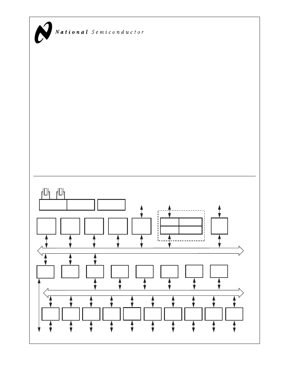
Block Diagram
CPU Core Bus
12 MHz and 32 kHz
Oscillator
Peripheral Bus
PLL and Clock
Generator
Power-on-Reset
Bus
Interface
Unit
Peripheral
Bus
Controller
Serial
Debug
Interface
DMA
Controller
Interrupt
Control
Unit
CVSD/PCM
Converter
Power
Manage-
ment
Timing and
Watchdog
Unit
8-Channel
12-bit ADC
Versatile
Timer Unit
Muti-Func-
tion Timer
Multi-Input
Wake-Up
GPIO
Audio
Interface
Microwiire/
SPI
Quad UART
Clock Generator
Protocol
Core
RF Interface
Bluetooth Lower
Link Controller
4.5K Bytes
Data RAM
1K Byte
Sequencer RAM
DS202
256K Bytes
Flash
Program
Memory
8K Bytes
Flash
Data
32K Bytes
Static
RAM
CR16C
CPU Core
ACCESS
.bus
CAN 2.0B
Controller
Random
Number
Generator
USB
Bluetooth is a registered trademark of Bluetooth SIG, Inc. and is used under license by National Semiconductor.
TRI-STATE is a registered trademark of National Semiconductor Corporation.
Document Outline
- 1.0 General Description
- 2.0 Features
- 3.0 Device Overview
- 3.1 CR16C CPU Core
- 3.2 Memory
- 3.3 Input/Output Ports
- 3.4 Bus Interface Unit
- 3.5 Interrupt Control Unit (ICU)
- 3.6 Multi-Input Wake-up
- 3.7 Bluetooth LLC
- 3.8 USB
- 3.9 CAN Interface
- 3.10 Quad UART
- 3.11 Advanced Audio interface
- 3.12 CVSD/PCM Conversion Module
- 3.13 12-bit Analog to Digital Converter
- 3.14 Random Number Generator
- 3.15 Microwire/SPI
- 3.16 ACCESS.bus Interface
- 3.17 Multi-Function Timer
- 3.18 Timing and Watchdog Module
- 3.19 Versatile Timer Unit
- 3.20 Triple Clock and Reset
- 3.21 Power Management
- 3.22 DMA Controller
- 3.23 Serial Debug Interface
- 3.24 Development Support
- 4.0 Signal Descriptions
- 5.0 CPU Architecture
- 6.0 Memory
- 7.0 System Configuration Registers
- 8.0 Flash Memory
- 9.0 DMA Controller
- 10.0 Interrupts
- 11.0 Triple Clock and Reset
- 12.0 Power Management
- 13.0 Multi-Input Wake-Up
- 14.0 Input/Output Ports
- 15.0 Bluetooth Controller
- 16.0 12-Bit Analog to Digital Converter
- 17.0 Random Number Generator (RNG)
- 18.0 USB Controller
- 19.0 CAN Module
- 20.0 Advanced Audio Interface
- 21.0 CVSD/PCM Conversion Module
- 22.0 UART Modules
- 23.0 Microwire/SPI Interface
- 24.0 ACCESS.bus Interface
- 25.0 Timing and Watchdog Module
- 26.0 Multi-Function Timer
- 27.0 Versatile Timer Unit (VTU)
- 28.0 Register Map
- 29.0 Register Bit Fields
- 30.0 Electrical Characteristics
- 30.1 Absolute Maximum Ratings
- 30.2 DC Electrical Characteristics (Temperature: -40˚C £ TA £ +85˚C)
- 30.3 USB Transceiver Electrical Characteristics (Temperature: -40˚C £ TA £ +85˚C)
- 30.4 ADC Electrical Characteristics (Temperature: -40˚C £ TA £ +85˚C)
- 30.5 Flash Memory On-Chip Programming
- 30.6 Output Signal Levels
- 30.7 Clock and Reset Timing
- 30.8 UART Timing
- 30.9 I/O Port Timing
- 30.10 Advanced Audio Interface (AAI) Timing
- 30.11 Microwire/SPI Timing
- 30.12 ACCESS.bus Timing
- 30.13 USB Port AC Characteristics
- 30.14 Multi-Function Timer (MFT) Timing
- 30.15 Versatile Timing Unit (VTU) Timing
- 30.16 External Bus Timing
- 31.0 Pin Assignments
- 32.0 Revision History
- 33.0 Physical Dimensions (millimeters) unless otherwise noted
