0 12-bit analog to digital converter, 1 functional description, Bit analog to digital converter – National CP3BT26 User Manual
Page 79: Functional description, Cp3 bt26

79
www.national.com
CP3
BT26
16.0 12-Bit Analog to Digital Converter
The integrated 12-bit ADC provides the following features:
8-input analog multiplexer
8 single-ended channels or 4 differential channels
External filtering capability
12-bit resolution with 11-bit accuracy
Sign bit
15-microsecond conversion time
Support for resistive touchscreen interface
Internal or external start trigger
Programmable start delay after start trigger
Poll or interrupt on done
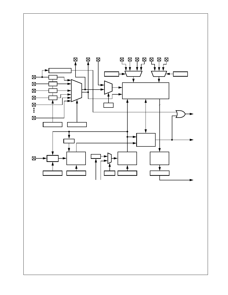
Figure 24.
Analog to Digital Converter Block Diagram
16.1
FUNCTIONAL DESCRIPTION
The ADC module consists of a 12-bit ADC converter and as-
sociated state machine, together with analog multiplexers to
set up signal paths for sampling and voltage references, log-
ic to control triggering of the converter, and a bus interface.
16.1.1
Data Path
Up to 8 GPIO pins may be configured as 8 singled-ended
analog inputs or 4 differential pairs. Analog/digital data
passes through four main blocks in the ADC module be-
tween the input pins and the CPU bus:
Input Multiplexer—an analog multiplexer that selects
among the input channels.
Internal/External Multiplexer—an analog multiplexer
that selects between the output of the Input Multiplexer
and the ADCIN external analog input.
12-Bit ADC—receives the output of the Internal/External
Multiplexer and performs the analog to digital conver-
sion.
ADCRESLT Register—makes conversion results from
the 12-Bit ADC available to the on-chip bus. The AD-
CRESLT register includes the software-visible end of a 4-
word FIFO used to queue conversion results.
The configuration of the analog signal paths is controlled by
fields in the ADCGCR register. The Input Multiplexer is con-
trolled by the MUX_CFG field. The Internal/External Multi-
plexer is controlled by the ADCIN bit. The analog
multiplexers for selecting the voltage references used by the
ADC are controlled by the PREF_CFG and NREF_CFG
fields. The low-ohmic drivers used for interface to resistive
touchscreens are controlled by the TOUCH_CFG field.
DS183
DRV
12-BIT ADC
MUXOUT0
ADC_DELAY1
DRV
Start
Interrupt
(IRQ13)
12
Done
System
Clock
ADC
SEQUENCER
VREFN
VREFP
+
-
TRIGGER
DELAY1
Auxiliary
Clock 2
MUXOUT1 ADCIN
CLKDIV
ASYNC
ADC7
TOUCH_CFG
MUX_CFG
ADC3/TSY+
DRV
ADC1/TSY-
ADC0/TSX+
ADC_DELAY2
DELAY2
DRV
ADC2/TSX-
ADC4
+
-
ADC2
ADC0
AVCC
ADC1
VREFP
ADC3
AGND
Control
Input
Multi-
plexer
Int/Ext
Multi-
plexer
ADC Clock
Pen-Down Detector
ADC_CONTROL
Result
Wake-Up
(WUI30)
ADCRESLT
4-Word
FIFO
System
Bus
Interface
Pen Down
CLKSEL
Clock
ADC_DIV
ADCIN
PREF_CFG
NREF_CFG
