0 bluetooth controller, 1 rf interface, Bluetooth controller – National CP3BT26 User Manual
Page 72: Rf interface, Cp3bt26

www.national.com
72
CP3BT26
15.0 Bluetooth Controller
The integrated hardware Bluetooth Lower Link Controller
(LLC) complies to the Bluetooth Specification Version 1.1
and integrates the following functions:
4.5K-byte dedicated Bluetooth data RAM
1K-byte dedicated Bluetooth Sequencer RAM
Support of all Bluetooth 1.1 packet types
Support for fast frequency hopping of 1600 hops/s
Access code correlation and slot timing recovery circuit
Power Management Control Logic
BlueRF-compatible interface to connect with National’s
LMX5252 and other RF transceiver chips
For a detailed description of the interface to the LMX5252,
consult the LMX5252 data sheet which is available from the
National Semiconductor wireless group. National provides
software libraries for using the Bluetooth LLC. Documenta-
tion for the software libraries is also available from National
Semiconductor.
15.1
RF INTERFACE
The CP3BT26 interfaces to the LMX5251 or LMX5252 radio
chips though the RF interface.
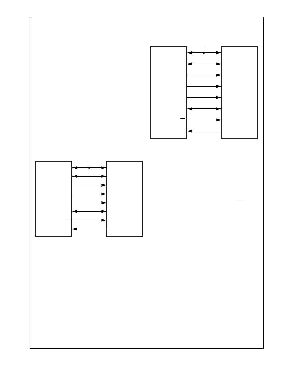
Figure 11 shows the interface between the CP3BT26 and
the LMX5251 radio chip.
Figure 11.
LMX5251 Interface
Figure 12 shows the interface between the CP3BT26 and
the LMX5252 radio chip.
Figure 12.
LMX5252 Interface
The CP3BT26 implements a BlueRF-compatible interface,
which may be used with other RF transceiver chips.
15.1.1
RF Interface Signals
The RF interface signals are grouped as follows:
Modem Signals (BBCLK, RFDATA, and RFSYNC)
Control Signal (RFCE)
Serial Interface Signals (SCLK, SDAT, and SLE)
Bluetooth Sequencer Status Signals (BTSEQ1,
BTSEQ2, and BTSEQ2)
X1CKI/BBCLK
The X1CKI/BBCLK pin is the input signal for the 12-MHz
clock signal. The radio chip uses this signal internally as the
12× oversampling clock and provides it externally to the
CP3BT26 for use as the Main Clock.
RFDATA
The RFDATA signal is the multiplexed Bluetooth data re-
ceive and transmit signal. The data is provided at a bit rate
of 1 Mbit/s with 12× oversampling, synchronized to the 12
MHz BBCLK. The RFDATA signal is a dedicated RF inter-
face pin. This signal is driven to a logic high level after reset.
RFSYNC
In receive mode (data direction from the radio chip to the
CP3BT26), the RFSYNC signal acts as the frequency cor-
rection/DC compensation circuit control output to the radio
chip. The RFSYNC signal is driven low throughout the cor-
relation phase and driven high when synchronization to the
received access code is achieved.
In transmit mode (data direction from the CP3BT26 to the
radio chip), the RFSYNC signal enables the RF output of
the radio chip. When the RFSYNC pin is driven high, the RF
CP3BT26
LMX5251
X1CKI/BBCLK
BBP_CLOCK
RFDATA
TX_RX_DATA
PG0/RFSYNC
TX_RX_SYNC
PG3/SCLK
CCB_CLOCK
PG4/SDAT
CCB_DATA
PG1/RFCE
CE
IOVCC
VDD_DIG_IN
VCC
PG5/SLE
CCB_LATCH
DS316
CP3BT26
LMX5252
X1CKI/BBCLK
BRCLK
RFDATA
BBDATA_1
PG2/BTSEQ1
BPKTCTL
PG3/SCLK
BDCLK
PG4/SDAT
BDDATA
PG1/RFCE
BXTLEN
IOVCC
VCC
+2.8V
PG5/SLE
BDEN#
DS320
