0 multi-function timer, 1 timer structure, Multi-function timer – National CP3BT26 User Manual
Page 196: Timer structure, Cp3bt26

www.national.com
196
CP3BT26
26.0 Multi-Function Timer
The Multi-Function Timer module contains a pair of 16-bit
timer/counters. Each timer/counter unit offers a choice of
clock sources for operation and can be configured to oper-
ate in any of the following modes:
Processor-Independent Pulse Width Modulation (PWM)
mode, which generates pulses of a specified width and
duty cycle, and which also provides a general-purpose
timer/counter.
Dual-Input Capture mode, which measures the elapsed
time between occurrences of external events, and which
also provides a general-purpose timer/counter.
Dual Independent Timer mode, which generates system
timing signals or counts occurrences of external events.
Single-Input Capture and Single Timer mode, which pro-
vides one external event counter and one system timer.
The timer unit uses two I/O pins, called TA and TB. The tim-
er I/O pins are alternate functions of the PG7 and PE4 port
pins, respectively.
26.1
TIMER STRUCTURE
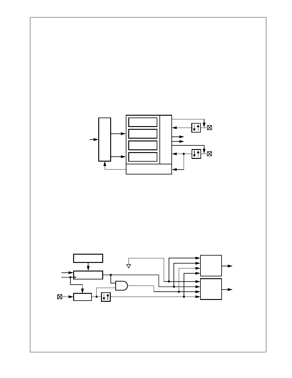
Figure 97 is a block diagram showing the internal structure
of the MFT. There are two main functional blocks: a Timer/
Counter and Action block and a Clock Source block. The
Timer/Counter and Action block contains two separate tim-
er/counter units, called Timer/Counter 1 and Timer/Counter
2.
Figure 97.
Multi-Function Timer Block Diagram
26.1.1
Timer/Counter Block
The Timer/Counter block contains the following functional
blocks:
Two 16-bit counters, Timer/Counter 1 (TCNT1) and Tim-
er/Counter 2 (TCNT2)
Two 16-bit reload/capture registers, TCRA and TCRB
Control logic necessary to configure the timer to operate
in any of the four operating modes
Interrupt control and I/O control logic
In a power-saving mode that uses the low-frequency
(32.768 kHz) clock as the System Clock, the synchroniza-
tion circuit requires that the Slow Clock operate at no more
than one-fourth the speed of the 32.768 kHz System Clock.
26.1.2
Clock Source Block
The Clock Source block generates the signals used to clock
the two timer/counter registers. The internal structure of the
Clock Source block is shown in Figure 98.
Figure 98.
Multi-Function Timer Clock Source
Reload/Capture A
TCRA
Timer/Counter
Clock Source
Action
TA
Interrupt B
Interrupt A
T
oggle/Capture/Interr
upt
Cloc
k Prescaler/Selector
Timer/Counter 1
TCNT1
Reload/Capture B
TCRB
Timer/Counter 2
TCNT2
PWM/Capture/Counter
Mode Select + Control
External Event
System
Clock
TB
DS081
Counter 1
Clock
Select
Counter 1
Clock
Counter 2
Clock
Select
Counter 2
Clock
Synchr.
External Event
Pulse Accumulator
5-Bit
Prescaler Counter
Prescaler Register
TPRSC
Reset
System
Clock
TB
Prescaled Clock
No Clock
DS082
