0 cpu architecture, 1 general-purpose registers, 2 dedicated address registers – National CP3BT26 User Manual
Page 15: Cpu architecture, General-purpose registers, Dedicated address registers, Cp3 bt26

15
www.national.com
CP3
BT26
5.0
CPU Architecture
The CP3BT26 uses the CR16C third-generation 16-bit
CompactRISC processor core. The CPU implements a Re-
duced Instruction Set Computer (RISC) architecture that al-
lows an effective execution rate of up to one instruction per
clock cycle. For a detailed description of the CPU16C archi-
tecture, see the CompactRISC CR16C Programmer’s Ref-
erence Manual which is available on the National
Semiconductor web site (http://www.nsc.com).
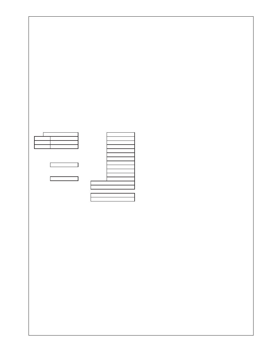
The CR16C CPU core includes these internal registers:
General-purpose registers (R0-R13, RA, and SP)
Dedicated address registers (PC, ISP, USP, and INT-
BASE)
Processor Status Register (PSR)
Configuration Register (CFG)
The R0-R11, PSR, and CFG registers are 16 bits wide. The
R12, R13, RA, SP, ISP and USP registers are 32 bits wide.
The PC register is 24 bits wide. Figure 2 shows the CPU
registers.
Figure 2.
CPU Registers
Some register bits are designated as “reserved.” Software
must write a zero to these bit locations when it writes to the
register. Read operations from reserved bit locations return
undefined values.
5.1
GENERAL-PURPOSE REGISTERS
The CompactRISC CPU features 16 general-purpose regis-
ters. These registers are used individually as 16-bit oper-
ands or as register pairs for operations on addresses
greater than 16 bits.
General-purpose registers are defined as R0 through
R13, RA, and SP.
Registers are grouped into pairs based on the setting of
the Short Register bit in the Configuration Register
(CFG.SR). When the CFG.SR bit is set, the grouping of
register pairs is upward-compatible with the architecture
of the earlier CR16A/B CPU cores: (R1,R0), (R2,R1) ...
(R11,R10), (R12_L, R11), (R13_L, R12_L), (R14_L,
R13_L) and SP. (R14_L, R13_L) is the same as
(RA,ERA).
When the CFG.SR bit is clear, register pairs are grouped
in the manner used by native CR16C software: (R1,R0),
(R2,R1) ... (R11,R10), (R12_L, R11), R12, R13, RA, SP.
R12, R13, RA, and SP are 32-bit registers for holding ad-
dresses greater than 16 bits.
With the recommended calling convention for the architec-
ture, some of these registers are assigned special hardware
and software functions. Registers R0 to R13 are for general-
purpose use, such as holding variables, addresses, or index
values. The SP register holds a pointer to the program run-
time stack. The RA register holds a subroutine return ad-
dress. The R12 and R13 registers are available to hold base
addresses used in the index addressing mode.
If a general-purpose register is specified by an operation
that is 8 bits long, only the lower byte of the register is used;
the upper part is not referenced or modified. Similarly, for
word operations on register pairs, only the lower word is
used. The upper word is not referenced or modified.
5.2
DEDICATED ADDRESS REGISTERS
The CR16C has four dedicated address registers to imple-
ment specific functions: the PC, ISP, USP, and INTBASE
registers.
5.2.1
Program Counter (PC) Register
The 24-bit value in the PC register points to the first byte of
the instruction currently being executed. CR16C instruc-
tions are aligned to even addresses, therefore the least sig-
nificant bit of the PC is always 0. At reset, the PC is
initialized to 0 or an optional predetermined value. When a
warm reset occurs, value of the PC prior to reset is saved in
the (R1,R0) general-purpose register pair.
5.2.2
Interrupt Stack Pointer (ISP)
The 32-bit ISP register points to the top of the interrupt
stack. This stack is used by hardware to service exceptions
(interrupts and traps). The stack pointer may be accessed
as the ISP register for initialization. The interrupt stack can
be located anywhere in the CPU address space. The ISP
cannot be used for any purpose other than the interrupt
stack, which is used for automatic storage of the CPU reg-
isters when an exception occurs and restoration of these
registers when the exception handler returns. The interrupt
stack grows downward in memory. The least significant bit
and the 8 most significant bits of the ISP register are always
0.
5.2.3
User Stack Pointer (USP)
The USP register points to the top of the user-mode pro-
gram stack. Separate stacks are available for user and su-
pervisor modes, to support protection mechanisms for
multitasking software. The processor mode is controlled by
the U bit in the PSR register (which is called PSR.U in the
shorthand convention). Stack grow downward in memory. If
the USP register points to an illegal address (any address
greater than 0x00FF_FFFF) and the USP is used for stack
access, an IAD trap is taken.
Dedicated Address Registers
23
31
PC
15
15
0
Processor Status Register
PSR
0
General-Purpose Registers
15
0
R0
R1
R2
R3
R4
R5
R6
R7
R8
R9
R10
R11
R12
R13
RA
SP
15
Configuration Register
CFG
0
ISPL
USPL
INTBASEL
ISPH
USPH
INTBASEH
31
DS004
