9 memory organization, Memory organization, Cp3 bt26 – National CP3BT26 User Manual
Page 127

127
www.national.com
CP3
BT26
19.9
MEMORY ORGANIZATION
The CAN module occupies 144 words in the memory ad-
dress space. This space is organized as 15 banks of 8
words per bank (plus one reserved bank) for the message
buffers and 14 words (plus 2 reserved words) for control and
status.
19.9.1
CPU Access to CAN Registers/Memory
All memory locations occupied by the message buffers are
shared by the CPU and CAN module (dual-ported RAM).
The CAN module and the CPU normally have single-cycle
access to this memory. However, if an access contention oc-
curs, the access to the memory is blocked every cycle until
the contention is resolved. This internal access arbitration is
transparent to software.
Both word and byte access to the buffer RAM are allowed.
If a buffer is busy during the reception of an object (copy
process from the hidden receive buffer) or is scheduled for
transmission, the CPU has no write access to the data con-
tents of the buffer. Write to the status/control byte and read
access to the whole buffer is always enabled.
All configuration and status registers can either be access-
ed by the CAN module or the CPU only. These registers pro-
vide single-cycle word and byte access without any
potential wait state.
All register descriptions within the next sections have the fol-
lowing layout:
19.9.2
Message Buffer Organization
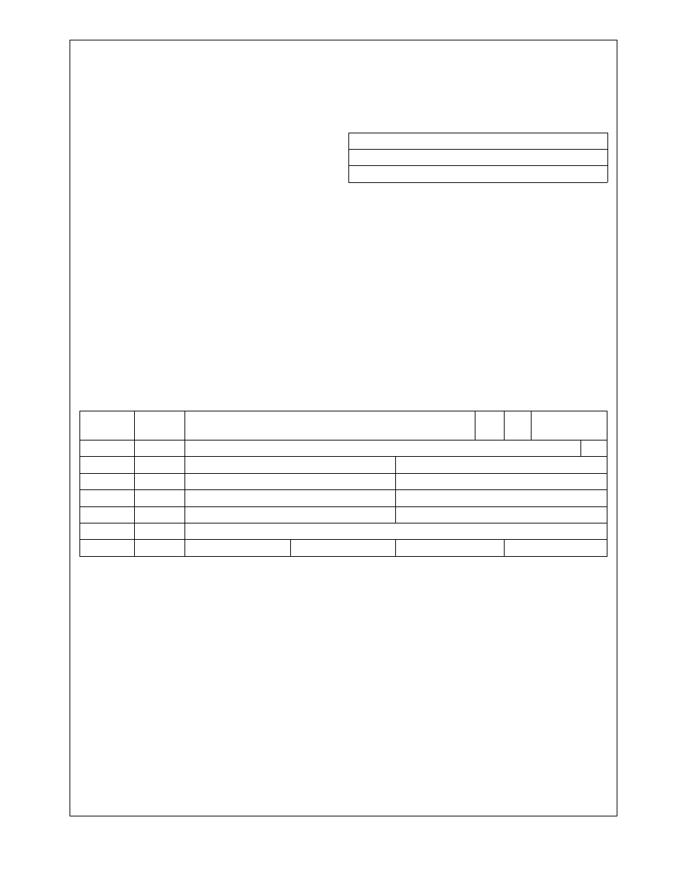
The message buffers are the communication interfaces be-
tween CAN and the CPU for the transmission and the re-
ception of CAN frames. There are 15 message buffers
located at fixed addresses in the RAM location. As shown in
Table 50, each buffer consists of two words reserved for the
identifiers, 4 words reserved for up to eight CAN data bytes,
one word reserved for the time stamp, and one word for data
length code, transmit priority code, and the buffer status
codes.
15
0
Bit/Field Names
Reset Value
CPU Access (R = read only, W = write only, R/W = read/write)
Table 50
Message Buffer Map
Address
Buffer
Register
15
14
13
12
11
10
9
8
7
6
5
4
3
2
1
0
0E F0XEh
ID1
XI[28:18]/ID[10:0]
SRR
/RTR
IDE
XI[17:15]
0E F0XCh
ID0
XI[14:0]
RTR
0E F0XAh
DATA0
Data1[7:0]
Data2[7:0]
0E F0X8h
DATA1
Data3[7:0]
Data4[7:0]
0E F0X6h
DATA2
Data5[7:0]
Data6[7:0]
0E F0X4h
DATA3
Data7[7:0]
Data8[7:0]
0E F0X2h
TSTP
TSTP[15:0]
0E F0X0h
CNSTAT
DLC
Reserved
PRI
ST
