5 system clock, 6 auxiliary clocks, 7 power-on reset – National CP3BT26 User Manual
Page 54: 8 external reset, 9 clock and reset registers, System clock, Auxiliary clocks, Power-on reset, External reset, Clock and reset registers

www.national.com
54
CP3BT26
11.5
SYSTEM CLOCK
The System Clock drives most of the on-chip modules, in-
cluding the CPU. Typically, it is driven by the Main Clock, but
it can also be driven by the PLL. In either case, the clock sig-
nal is passed through a programmable divider (scale factors
from ÷1 to ÷16).
11.6
AUXILIARY CLOCKS
Auxiliary Clock 1 and Auxiliary Clock 2 are generated from
Main Clock for use by certain peripherals. Auxiliary Clock 1
is available for the Bluetooth controller and the Advanced
Audio Interface. Auxiliary Clock 2 is available for the CVSD/
PCM transcoder and the 12-bit ADC. The Auxiliary clocks
may be configured to keep these peripherals running when
the System Clock is slowed down or suspended during low-
power modes.
11.7
POWER-ON RESET
The Power-On Reset circuit generates a system reset signal
at power-up and holds the signal active for a period of time
to allow the crystal oscillator to stabilize. The circuit detects
a power turn-on condition, which presets a 14-bit timer driv-
en by Main Clock to a value of 3FFFh. This preset value is
defined in hardware and not programmable. Once oscilla-
tion starts and the clock becomes active, the timer starts
counting down. When the count reaches zero, the 14-bit
timer stops counting and the internal reset signal is deacti-
vated (unless the RESET pin is held low).
The circuit sets a power-on reset bit on detection of a power-
on condition. The CPU can read this bit to determine wheth-
er a reset was caused by a power-up or by the RESET input.
Note: The Power-On Reset circuit cannot be used to detect
a drop in the supply voltage.
11.8
EXTERNAL RESET
The active-low RESET input can be used to reset the device
at any time. When the signal goes low, it generates an inter-
nal system reset signal that remains active until the RESET
signal goes high again. There is no internal pullup on this in-
put, so it must be driven or pulled high externally for proper
device operation.
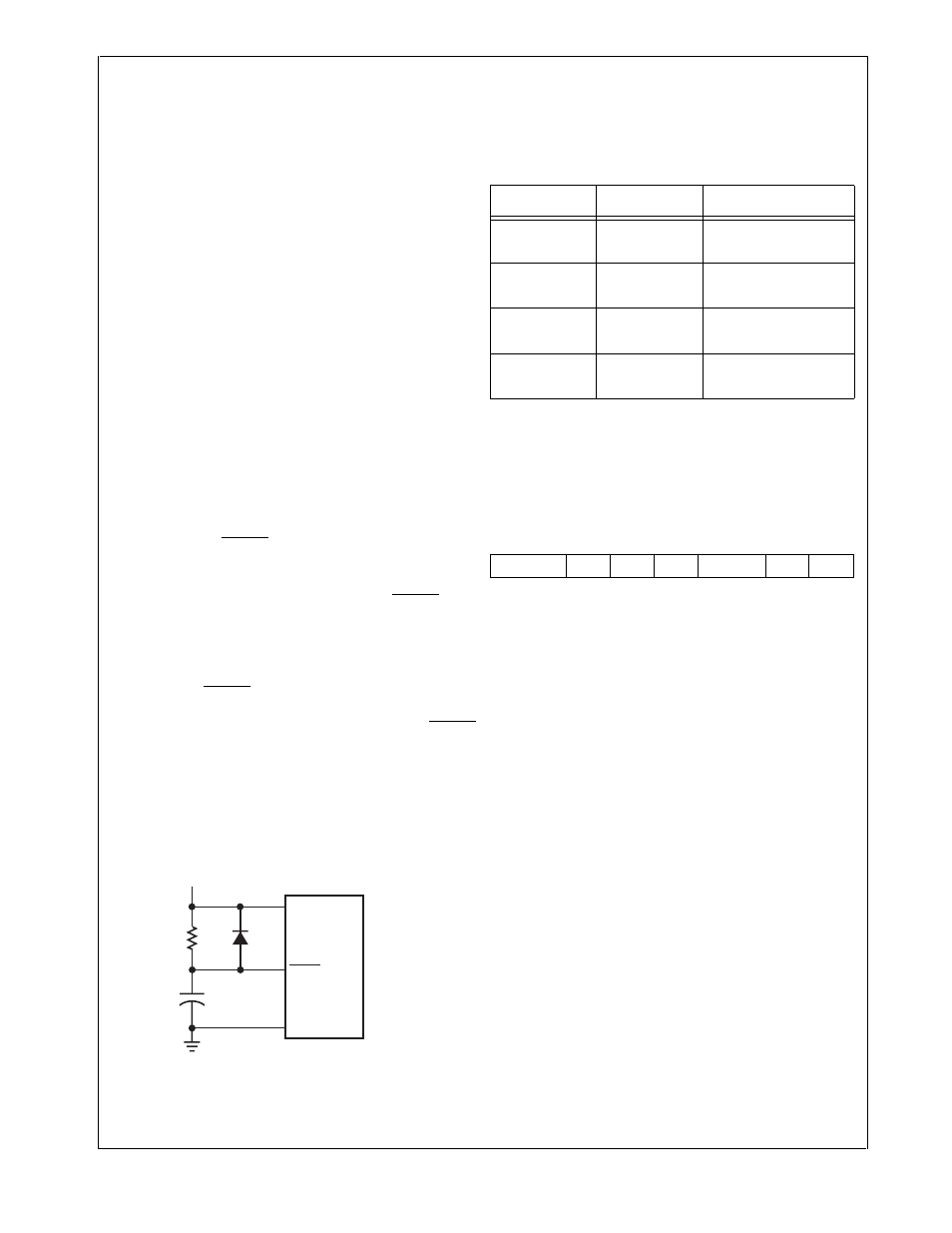
If the VCC power supply has slow rise-time. it may be nec-
essary to use an external reset circuit to insure proper de-
vice initialization. Figure 7 shows an example of an external
reset circuit.
Figure 7.
External Reset Circuit
The value of R should be less than 50K ohms. The RC time
constant of the circuit should be 5 times the power supply
rise time. The time constant also should exceed the stabili-
zation time for the high-frequency oscillator.
11.9
CLOCK AND RESET REGISTERS
Table 23 lists the clock and reset registers.
11.9.1
Clock and Reset Control Register (CRCTRL)
The CRCTRL register is a byte-wide read/write register that
controls the clock selection and contains the power-on reset
status bit. At reset, the CRCTRL register is initialized as de-
scribed below:
SCLK
The Slow Clock Select bit controls the clock
source used for the Slow Clock.
0
–
Slow Clock driven by prescaled Main
Clock.
1
–
Slow Clock driven by 32.768 kHz oscilla-
tor.
FCLK
The Fast Clock Select bit selects between the
12 MHz Main Clock and the PLL as the source
used for the System Clock. After reset, the
Main Clock is selected. Attempting to switch to
the PLL while the PLLPWD bit is set (PLL is
turned off) is ignored. Attempting to switch to
the PLL also has no effect if the PLL output
clock has not stabilized.
0
–
The System Clock prescaler is driven by
the output of the PLL.
1
–
The System Clock prescaler is driven by
the 12-MHz Main Clock. This is the de-
fault after reset.
PLLPWD
The PLL Power-Down bit controls whether the
PLL is active or powered down (Stop PLL sig-
nal asserted). When this bit is set, the on-chip
PLL stays powered-down. Otherwise it is pow-
ered-up or it can be controlled by the Power
Management Module, respectively. Before
software can power-down the PLL in Active
mode by setting the PLLPWD bit, the FCLK bit
must be set. Attempting to set the PLLPWD
bit while the FCLK bit is clear is ignored. The
GND
IOVCC
RESET
DS216
CP3BT2x
IOVCC
R
C
Table 23
Clock and Reset Registers
Name
Address
Description
CRCTRL
FF FC40h
Clock and Reset
Control Register
PRSFC
FF FC42h
High Frequency Clock
Prescaler Register
PRSSC
FF FC44h
Low Frequency Clock
Prescaler Register
PRSAC
FF FC46h
Auxiliary Clock
Prescaler Register
7
6
5
4
3
2
1
0
Reserved
POR ACE2 ACE1 PLLPWD FCLK SCLK
