Cp3bt26 – National CP3BT26 User Manual
Page 182

www.national.com
182
CP3BT26
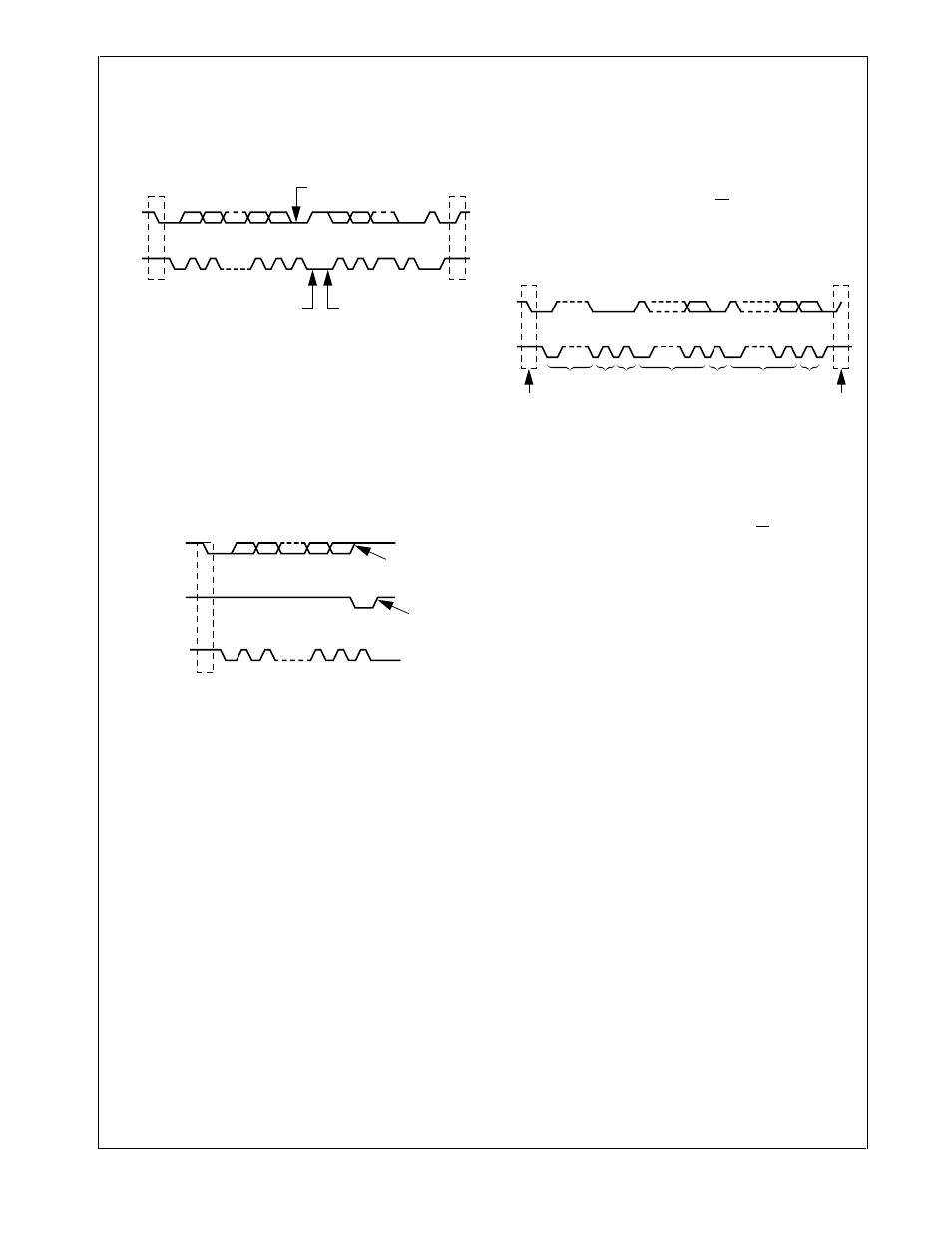
Acknowledge Cycle
The Acknowledge Cycle consists of two signals: the ac-
knowledge clock pulse the master sends with each byte
transferred, and the acknowledge signal sent by the receiv-
ing device (Figure 93).
Figure 93.
ACCESS.bus Data Transaction
The master generates the acknowledge clock pulse on the
ninth clock pulse of the byte transfer. The transmitter releas-
es the SDA line (permits it to go high) to allow the receiver
to send the acknowledge signal. The receiver must pull
down the SDA line during the acknowledge clock pulse,
which signals the correct reception of the last data byte, and
its readiness to receive the next byte. Figure 94 illustrates
the acknowledge cycle.
Figure 94.
ACCESS.bus Acknowledge Cycle
The master generates an acknowledge clock pulse after
each byte transfer. The receiver sends an acknowledge sig-
nal after every byte received. There are two exceptions to
the “acknowledge after every byte” rule.
When the master is the receiver, it must indicate to the
transmitter an end-of-data condition by not-acknowledg-
ing (“negative acknowledge”) the last byte clocked out of
the slave. This “negative acknowledge” still includes the
acknowledge clock pulse (generated by the master), but
the SDA line is not pulled down.
When the receiver is full, otherwise occupied, or a prob-
lem has occurred, it sends a negative acknowledge to in-
dicate that it cannot accept additional data bytes.
Addressing Transfer Formats
Each device on the bus has a unique address. Before any
data is transmitted, the master transmits the address of the
slave being addressed. The slave device should send an
acknowledge signal on the SDA signal, once it recognizes
its address.
The address is the first seven bits after a Start Condition.
The direction of the data transfer (R/W) depends on the bit
sent after the address (the eighth bit). A low-to-high transi-
tion during a SCL high period indicates the Stop Condition,
and ends the transaction (Figure 95).
Figure 95.
A Complete ACCESS.bus Data Transaction
When the address is sent, each device in the system com-
pares this address with its own. If there is a match, the de-
vice considers itself addressed and sends an acknowledge
signal. Depending upon the state of the R/W bit (1 = read,
0 = write), the device acts as a transmitter or a receiver.
The ACCESS.bus protocol allows sending a general call ad-
dress to all slaves connected to the bus. The first byte sent
specifies the general call address (00h) and the second byte
specifies the meaning of the general call (for example,
“Write slave address by software only”). Those slaves that
require the data acknowledge the call and become slave re-
ceivers; the other slaves ignore the call.
Arbitration on the Bus
Arbitration is required when multiple master devices attempt
to gain control of the bus simultaneously. Control of the bus
is initially determined according to address bits and clock
cycle. If the masters are trying to address the same bus de-
vice, data comparisons determine the outcome of this arbi-
tration. In master mode, the device immediately aborts a
transaction if the value sampled on the SDA lines differs
from the value driven by the device. (Exceptions to this rule
are SDA while receiving data; in these cases the lines may
be driven low by the slave without causing an abort.)
The SCL signal is monitored for clock synchronization and
allows the slave to stall the bus. The actual clock period will
be the one set by the master with the longest clock period
or by the slave stall period. The clock high period is deter-
mined by the master with the shortest clock high period.
When an abort occurs during the address transmission, the
master that identifies the conflict should give up the bus,
switch to slave mode, and continue to sample SDA to see if
it is being addressed by the winning master on the AC-
CESS.bus.
SDA
S
1
MSB
ACK
ACK
Stop
Condition
Start
Condition
Clock Line Held
Low by Receiver
While Interrupt
is Serviced
Byte Complete
Interrupt Within
Receiver
Acknowledgment
Signal from Receiver
SCL
2
1
2
3-8
7
3 - 6
8
9
9
P
DS077
1
Transmitter Stays Off
the Bus During the
Acknowledgment Clock
Acknowledgment
Signal from Receiver
Data Output
by Transmitter
Data Output
by Receiver
SCL
2
7
3 - 6
8
9
S
Start
Condition
DS078
SDA
1 - 7
ACK
Data
Address
SCL
S
Stop
Condition
Start
Condition
P
8
9
1 - 7
8
9
1 - 7
8
9
R/W
Data
ACK
ACK
DS079
