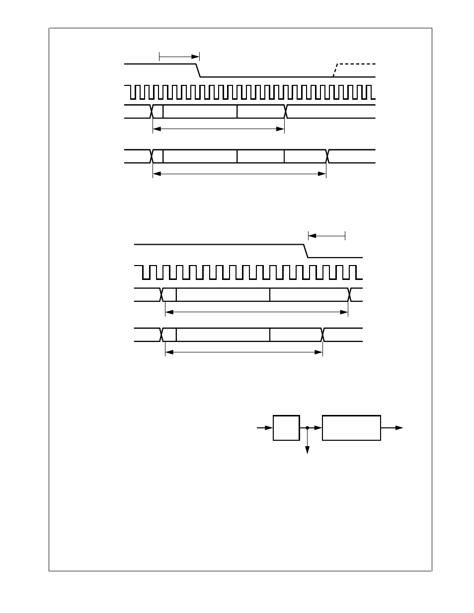
3 message transfer, Message transfer, Sjw (see figure 45 – National CP3BT26 User Manual
Page 118: See figure 46, Cp3bt26

www.national.com
118
CP3BT26
Figure 45.
Resynchronization (e > SJW)
Figure 46.
Resynchronization (e < -SJW)
19.2.7
Clock Generator
The CAN prescaler (PSC) is shown is Figure 47. It divides
the CKI input clock by the value defined in the CTIM register.
The resulting clock is called time quanta clock and defines
the length of one time quantum (tq).
Please refer to CAN Timing Register (CTIM) on page 135
for a detailed description of the CTIM register.
Note: PSC is the value of the clock prescaler. TSEG1 and
TSEG2 are the length of time segment 1 and 2 in time quan-
ta.
The resulting bus clock can be calculated by the equation:
The values of PSC, TSEG1, and TSEG2 are specified by
the contents of the registers PSC, TSEG1, and TSEG2 as
follows:
PSC = PSC[5:0] + 2
TSEG1 = TSEG1[3:0] + 1
TSEG2 = TSEG2[2:0] + 1
Figure 47.
CAN Prescaler
19.3
MESSAGE TRANSFER
The CAN module has access to 15 independent message
buffers, which are memory mapped in RAM. Each message
buffer consists of 8 different 16-bit RAM locations and can
be individually configured as a receive message buffer or as
a transmit message buffer.
A dedicated acceptance filtering procedure enables soft-
ware to configure each buffer to receive only a single mes-
sage ID or a group of messages. One buffer uses an
Bus
Signal
PREVIOUS
BIT
"NORMAL" BIT TIME
NEXT BIT
TSEG2
TSEG1
A
e
PREVIOUS
BIT
NEXT BIT
TSEG2
SJW
TSEG1
A
BIT TIME LENGTHENED BY SJW
CAN
Clock
DS029
PREVIOUS
BIT
"NORMAL" BIT TIME
TSEG2
TSEG1
A
e
PREVIOUS
BIT
BIT TIME SHORTENED BY SJW
NEXT BIT
TSEG2
TSEG1
A
Bus
Signal
CAN
Clock
DS030
busclock
CKI
PSC
(
)x 1 TSEG1 TSEG2
+
+
(
)
-------------------------------------------------------------------------------------
=
PSC
CKI
Bit Rate
Internal Time
Quanta Clock (1/tq)
÷
(1+TSEG1+TSEG2)
÷
DS031
