0 input/output ports, 1 port registers, Input/output ports – National CP3BT26 User Manual
Page 67: Port registers, Cp3 bt26

67
www.national.com
CP3
BT26
14.0 Input/Output Ports
Each device has up to 54 software-configurable I/O pins, or-
ganized into 8-bit ports (not all bits are used in some ports).
The ports are named Port B, Port C, Port E, Port F, Port G,
Port H, and Port J.
In addition to their general-purpose I/O capability, the I/O
pins of Ports E, F, G, H, and J have alternate functions for
use with on-chip peripheral modules such as the UART or
the Multi-Input Wake-Up unit. The alternate functions of all
I/O pins are shown in Table 94.
Ports B and C are used as the 16-bit data bus when an ex-
ternal bus is enabled (144-pin devices only). This alternate
function is selected by enabling the DEV or ERE operating
environments, not by programming the port registers.
The I/O pin characteristics are fully programmable. Each pin
can be configured to operate as a TRI-STATE output, push-
pull output, weak pull-up input, or high-impedance input.
Different pins within the same port can be individually con-
figured to operate in different modes.
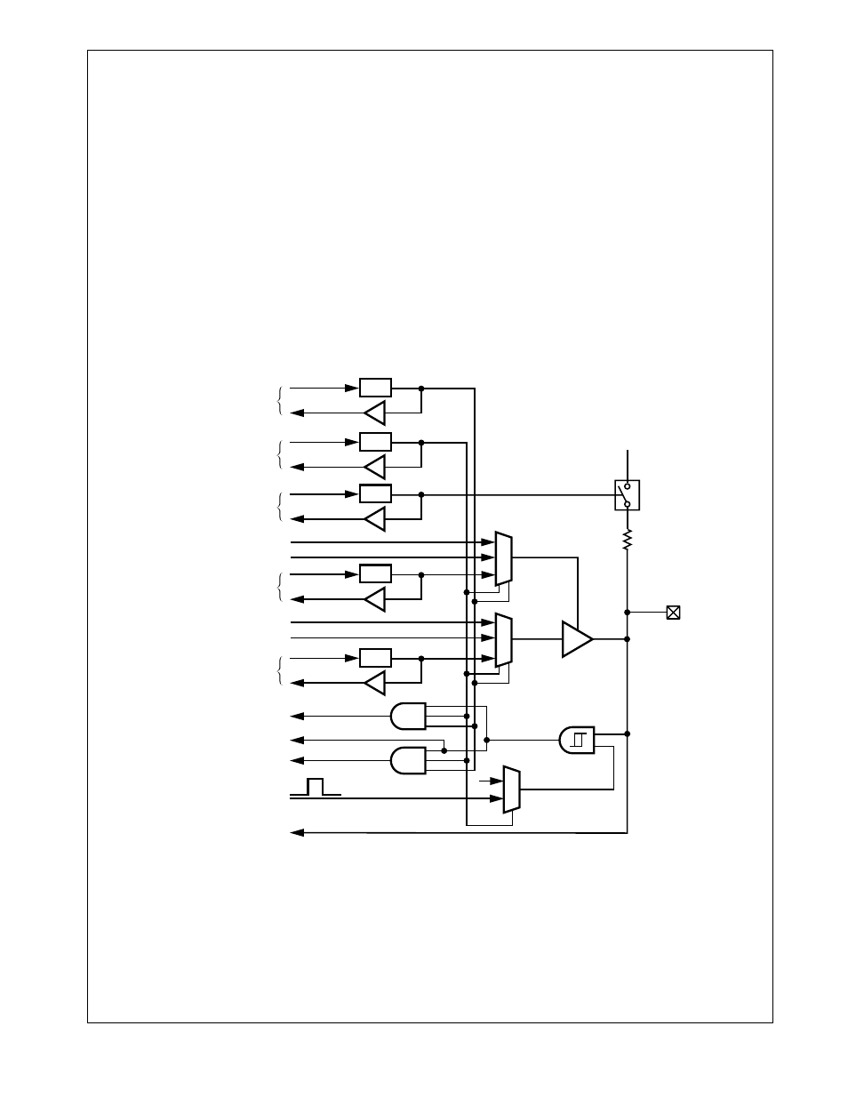
Figure 10 is a diagram showing the I/O port pin logic. The
register bits, multiplexers, and buffers allow the port pin to
be configured into the various operating modes. The output
buffer is a TRI-STATE buffer with weak pull-up capability.
The weak pull-up, if used, prevents the port pin from going
to an undefined state when it operates as an input.
To reduce power consumption, input buffers configured for
general-purpose I/O are only enabled when they are read.
When configured for an alternate function, the input buffers
are enabled continuously. To minimize power consumption,
input signals to enabled buffers must be held within 0.2 volts
of the VCC or GND voltage.
The electrical characteristics and drive capabilities of the in-
put and output buffers are described in Section 30.0.
Figure 10.
I/O Port Pin Logic
14.1
PORT REGISTERS
Each port has an associated set of memory-mapped regis-
ters used for controlling the port and for holding the port da-
ta:
PxALT: Port alternate function register
PxALTS: Port alternate function select register
PxDIR: Port direction register
PxDIN: Port data input register
PxDOUT: Port data output register
PxWPU: Port weak pull-up register
PxHDRV: Port high drive strength register
Data In Read Strobe
Alt. A Device Direction
Alt. B Device Direction
Alt. B Data Input
Analog Input
PxDIN Register
PxALTS Register
PxALT Register
PxWKPU Register
PxDIR Register
Alt. A Device Data Outout
Alt. B Device Data Outout
PxDOUT Register
1
DS190
Alt. A Data Input
VCC
Weak Pull-Up Enable
Output Enable
Data Out
Pin
Data In
D
Q
D
Q
D
Q
D
Q
D
Q
