2 touchscreen interface, Touchscreen interface, Cp3 bt26 – National CP3BT26 User Manual
Page 81

81
www.national.com
CP3
BT26
16.2
TOUCHSCREEN INTERFACE
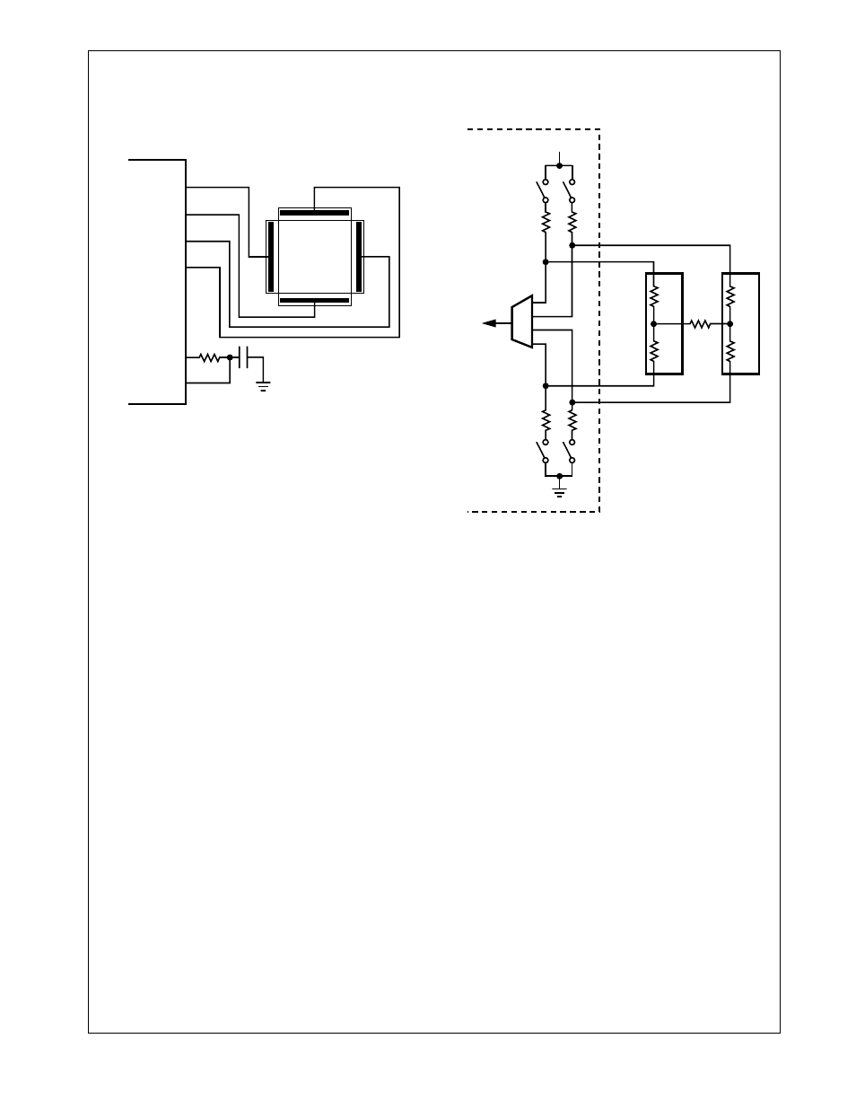
The ADC provides an interface for 4-wire resistive touch-
screens with the resolution necessary for applications such
as signature analysis. A typical touchscreen configuration is
shown in Figure 25.
Figure 25.
Touchscreen Interface
A touchscreen consists of two resistive plates normally sep-
arated from each other. The TSX+ and TSX- signals are
connected to opposite ends of the X plate, while the TSY+
and TSY- signals are connected to the Y plate. If the pen is
down, the plates will be shorted together at the point of pen
contact. The location of the pen is sensed by driving one
end of a plate to VCC, driving the opposite end to ground,
and sensing the voltage at the point of pen contact using the
other plate. This is done twice, once for each coordinate.
An external RC low-pass filter is used to remove noise cou-
pled to the touchscreen signals from the display drivers.
16.2.1
Touchscreen Driver Configuration
An equivalent circuit for the touchscreen interface is shown
in Figure 26.
Figure 26.
Touchscreen Driver Equivalent Circuit
Low-ohmic drivers are provided to pull the TSX+ and TSY+
signals to VCC and the TSX- and TSY- signals to GND. The
on-resistance of these drivers is specified to be 6 ohms.
Two measurements are used to produce one (x,y) position
coordinate pair. To measure the x-coordinate, the TSX+ sig-
nal is pulled to VCC, the TSX- signal is pulled to GND, and
the TSY+ and TSY- signals are undriven. A voltage divider
is formed across the X plate, with the center tap of the divid-
er being the point of pen contact, represented in Figure 26
by node A. With TSY+ and TSY- undriven, the voltage at
node A can be measured by sampling either of the TSY+ or
TSY- signals. This voltage will be proportional to the position
of the pen contact on the X plate.
The position of the pen contact on the Y plate is measured
similarly, by driving the TSY+ signal to VCC, the TSY- signal
to GND, and leaving the TSX+ and TSX- signals undriven.
The voltage at node B can be sampled from either the TSX+
or TSX- signals. The TOUCH_CFG field of the ADCGCR
register specifies the configuration of the drivers, with 010b
used to sample node A and 001b used to sample node B.
Typically, two consecutive measurements are made of each
coordinate so that any interference coupled from the LCD
column drivers is averaged out.
The plate-to-plate resistance is shown in Figure 26 as RZ.
This measurement is used as an indication of the force of
pen contact. When 100b is loaded into the TOUCH_CFG
field, the TSY+ signal is pulled to VCC and the TSX- signal
is pulled to GND, to support measuring RZ.
DS186
TSX+/ADC0
TSY+/ADC1
TSX-/ADC2
TSY-/ADC3
MUXOUT0
ADCIN
DS187
6
Ω
6
Ω
6
Ω
6
Ω
RX1
RZ
X Plate
TSY
+
TSX
+
TSX
-
To ADC
TSY
-
RX2
A
VCC
RY1
Y Plate
RY2
B
