5 bluetooth sleep mode, 6 bluetooth global registers, 7 bluetooth sequencer ram – National CP3BT26 User Manual
Page 77: Bluetooth sleep mode, Bluetooth global registers, Bluetooth sequencer ram, Cp3 bt26

77
www.national.com
CP3
BT26
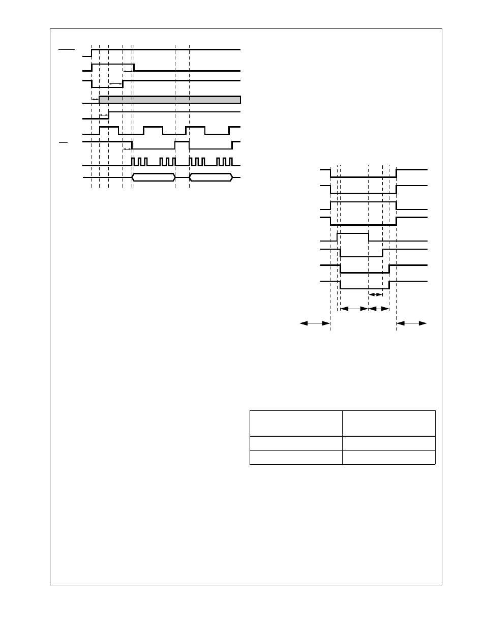
Figure 22.
LMX5252 Power-Up Sequence
15.5
BLUETOOTH SLEEP MODE
The Bluetooth controller is capable of putting itself into a
sleep mode for a specified number of Slow Clock cycles. In
this mode, the controller clocks are stopped internally. The
only circuitry which remains active are two counters
(counter N and counter M) running at the Slow Clock rate.
These counters determine the duration of the sleep mode.
The sequence of events when entering the LLC sleep mode
is as follows:
1. The current Bluetooth counter contents are read by the
CPU.
2. Software “estimates” the Bluetooth counter value after
leaving the sleep mode.
3. The new Bluetooth counter value is written into the
Bluetooth counter register.
4. The Bluetooth sequencer RAM is updated with the
code required by the Bluetooth sequencer to enter/exit
Sleep mode.
5. The Bluetooth sequencer RAM and the Bluetooth LLC
registers are switched from the System Clock domain
to the local 12 MHz Bluetooth clock domain. At this
point, the Bluetooth sequencer RAM and Bluetooth
LLC registers cannot be updated by the CPU, because
the CPU no longer has access to the Bluetooth LLC.
6. Hardware Clock Control (HCC) is enabled, and the
CP3BT26 enters a power-saving mode (Power Save or
Idle mode). While in Power Save mode, the Slow Clock
is used as the System Clock. While in Idle mode, the
System Clock is turned off.
7. The Bluetooth sequencer checks if HCC is enabled. If
HCC is enabled, the sequencer asserts HCC to the
PMM. On the next rising edge of the low-frequency
clock, the 1MHz clock and the 12 MHz clock are
stopped locally within the Bluetooth LLC. At this point,
the Bluetooth sequencer is stopped.
8. The M-counter starts counting. After M + 1 Slow Clock
cycles, the HCC signal to the PMM is deasserted.
9. The PMM restarts the 12 MHz Main Clock (and the
PLL, if required). The N-counter starts counting. After
N + 1 Slow Clock cycles, the Bluetooth clocks (1 MHz
and 12 MHz) are turned on again. The Bluetooth se-
quencer starts operating.
10. The Bluetooth sequencer waits for the completion of
the sleep mode. When completed, the Bluetooth se-
quencer asserts a wake-up signal to the MIWU (see
Section 13.0).
11. The PMM switches the System Clock to the high-fre-
quency clock and the CP3BT26 enters Active mode
again. HCC is disabled. The Bluetooth sequencer RAM
and Bluetooth LLC registers are switched back from the
local 12 MHz Bluetooth clock to the System Clock. At
this point, the Bluetooth sequencer RAM and Bluetooth
LLC registers are once again accessible by the CPU. If
enabled, an interrupt is issued to the CPU.
Figure 23.
Bluetooth Sleep Mode Sequence
15.6
BLUETOOTH GLOBAL REGISTERS
Table 32 shows the memory map of the Bluetooth LLC glo-
bal registers.
Table 32
Memory Map of Bluetooth Global Registers
15.7
BLUETOOTH SEQUENCER RAM
The sequencer RAM is a 1K memory-mapped section of
RAM that contains the sequencer program. This RAM can
be read and written by the CPU in the same way as the Stat-
ic RAM space and can also be read by the sequencer in the
Bluetooth LLC. Arbitration between these devices is per-
formed in hardware.
BBCLK
t1
RESET
DS321
SDAT
SCLK
B3k2
BPOR
t2
RFCE
t3
t4
RFDATA
t5
SLE
Address
(offset from 0E F180h)
Description
0000h
–
0048h
Global LLC Configuration
0049h
–
007Fh
Unused
Active
Power Save
CPU
Active
Stopped/Slow
System Clock
System Clock
Main Clock
BT LCC Clock
Active
Stopped
12 MHz
Main Clock
Active
Stopped
1 MHz/12 MHz
BT Clock
Active
Stopped
Sequencer
Enabled
Disabled
HCC
Asserted
Deasserted
HCC
N
M
Start-up
CPU Handles
Wake-Up IRQ
from MIWU
CPU
Prepare for
Sleep Mode
DS017
