2 physical description – Comtech EF Data CDM-710G User Manual
Page 176
CDM-710G High-Speed Satellite Modem
Revision 1
HSSI Interface (CDI-60)
MN-CDM710G
13–2
13.2
Physical Description
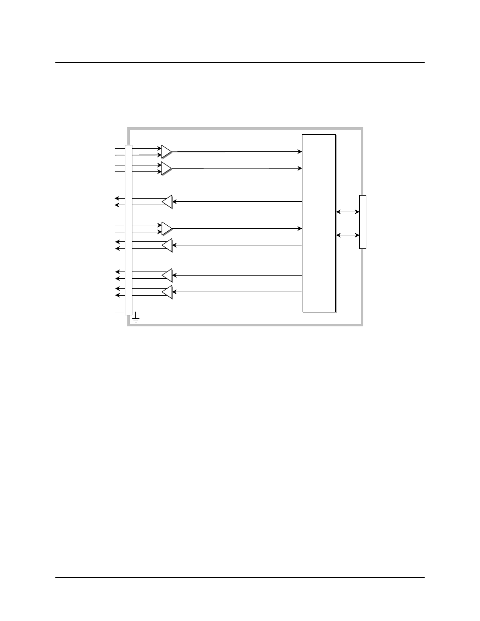
Figure 13-2 depicts the block diagram for the interface. The HSSI data interface is implemented
on a 3.95 x 7.022 inch (10.03 x 17.83 cm) PCB. Connection to the modem is provided when the
96-pin DIN connector is engaged into the modem slot.
Figure 13-2. CDI-60 HSSI Data Interface Module Block Diagram
Figure 13-3 shows the CDI-60 HSSI interface, looking towards the real panel. The 50-pin
SCSI-2 connector serves as the data port, and a Light-Emitting Diode (LED), labeled Activity, is
lit green when the interface is enabled.
The CDI-60 HSSI interface provides:
• A single HSSI interface;
• DCE Connection;
• ST clock is sourced to the terrestrial interface for use as reference by DTE;
• TT is treated as an incoming External Clock, and the interface phase locks to it;
• TA / CA is supported.
The connector pinout for the interface is provided in Sect. 13-3; a summary of specifications for the
interface is provided in Sect. 13-4.
Processor
Mux /
Demux
PLL
Rx
Buffer
Interface
Loopback
Control
Processor
Mux /
Demux
PLL
Rx
Buffer
Interface
Loopback
Control
Modem
Interface
Clk
&
Data
μC
HSSI Interface
TT
SD
ST
Common
J1
Rx Clock
Rx Data
50 Pi
n
H
S
S
I Fem
al
e
TA
CA
(RTS)
(CTS)
Tx Clock Input (External)
Tx Data
Output Clock (Rate Programmable)
RT
RD