2 physical description – Comtech EF Data CDM-710G User Manual
Page 172
CDM-710G High-Speed Satellite Modem
Revision 1
Single G.703 (E3/T3/STS-1) Interface (CDI-10-1)
MN-CDM710G
12–2
UNBAL
UNBAL
G.703
E1/T1
E2/T2
G.703
E1/T1
E2/T2
Ext
BAL
Clock
Ext
BAL
Clock
UNBAL
E3/T3/STS
-
1
Processor
Mux /
Demux
PLLs
Rx
Buffers
Interface
Loopback
Processor
Mux /
Demux
PLLs
Rx
Buffers
Interface
Loopback
Modem
Interface
Tx
Rx
Clk
&
Data
μ
C
BNC Female 3 Places
J3
J2
Single E3/T3/STS
-
1 Card
Loopback
EXT Clk
J1
External Clock
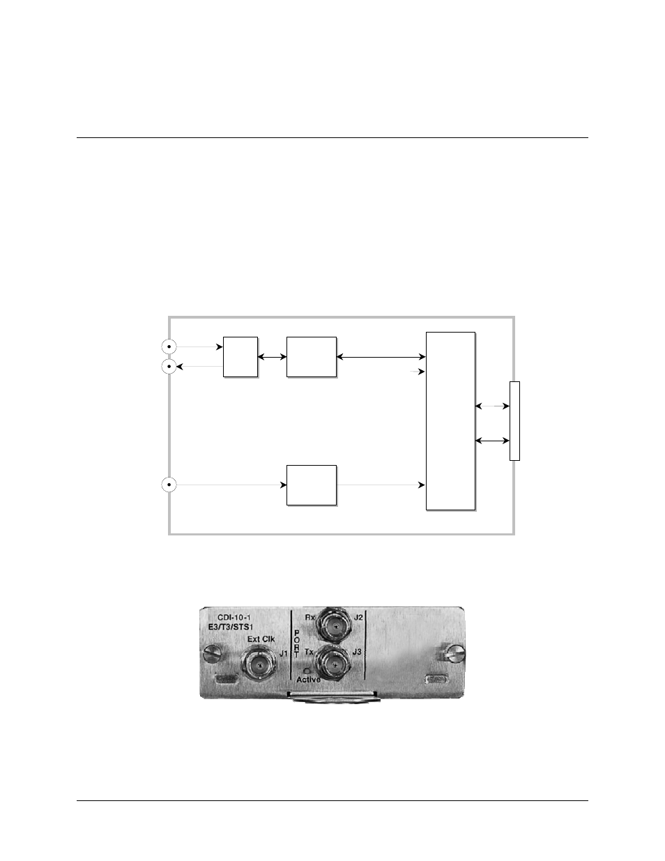
For a table of the applicable interfaces and installable combinations, refer to Sect. 1.3.5 Allowable
Data Interface Combinations.
12.2
Physical Description
Figure 12-2 depicts the block diagram of the interface; Figure 12-3 shows the rear panel of the
interface. The data interfaces provided here are as follows (left to right):
• External Clock Input Port (J1)
• The CDI-10-1 module provides a Single G.703 Interface Port – Rx / J2 (top) and Tx / J3
(bottom) – that is operable/selectable as E3, T3, STS-1 or OFF.
Additionally, a Light-Emitting Diode (LED) labeled Active lights when G.703 data activity is
sensed.
Refer to the next section for connector information.
Figure 12-2. CDI-10-1 Block Diagram
Figure 12-3. CDI-10-1 Rear Panel View