Reset structure, Error flagging and handling, Spi-4.2 error detection and handling – Altera POS-PHY Level 4 IP Core User Manual
Page 81
Chapter 5: Functional Description—Transmitter
5–11
Reset Structure
December 2014
Altera Corporation
POS-PHY Level 4 IP Core User Guide
1
The SPI-4.2 tdclk is not a separate clock domain because it is not on an FPGA clock
signal. Instead, alternating 1s and 0s are preloaded into the tdclk serializer. As tdclk
is generated using the same PLL as the rest of the data, the clock and data are
launched at the same time. The same technique applies to the 32-bit data path width,
where the ALTLVDS IP core is set to alternating 1s and 0s for the tdclk signal.
Reset Structure
By default, the txreset_n signal is the asynchronous global reset for the IP core. It is
internally metastable hardened and passed to each of the individual clock domains.
Asserting reset deletes all data in the buffers and resets all of the state bits in the error
checking logic.
In addition to the reset, asynchronous reset and locked signals are provided for the
internal PLL, if present. The PLL should be reset and stable along with all other clocks
before the reset is released.
Error Flagging and Handling
This section outlines how the POS-PHY Level 4 transmitter IP core responds to
various errors.
SPI-4.2 Error Detection and Handling
The transmitter IP core monitors and decodes the SPI-4.2 input status channel. When
an error is detected, an error flag is asserted. The flag pulses high for one tsclk period
for each error. Errors occur when the received status channel does not match
expectations set by the state machine shown in Figure 6.11 FIFO Status State Diagram
(Sending Side) of the SPI-4.2 Specification.
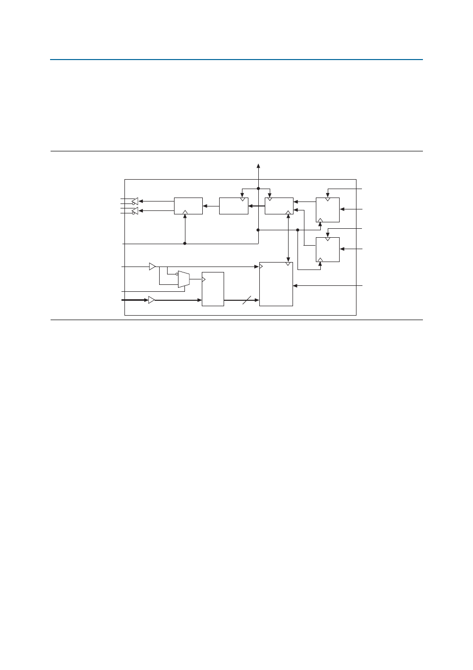
Figure 5–5. Clock Layout Diagram (Quarter Rate)
Data
Processor
LVTTL
LVTTL
Status
Processor
Scheduler
Atlantic
Buffer 0
Atlantic
Interface 0
a0_atxclk
aN_atxclk
(Note 2, 3)
tdat[15:0]
tctl
tdclk
txsys_clk
tdint_clk
altddio_out
tsclk
ctl_ts_statedge
trefclk
tstat[1:0]
Atlantic
Buffer N
Atlantic
Interface N
2