Lvds data rate – Altera POS-PHY Level 4 IP Core User Manual
Page 22
3–2
Chapter 3: Parameter Settings
Basic Parameters
POS-PHY Level 4 IP Core User Guide
December 2014
Altera Corporation
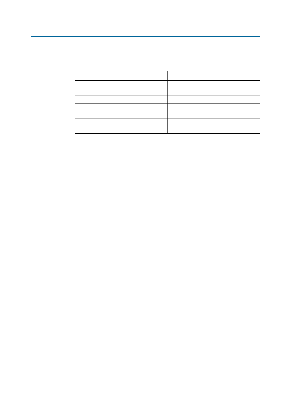
Table 3–1
shows the maximum LVDS data rates supported by the POS-PHY Level 4 IP
core for each device family.
The POS-PHY Level 4 IP core operates either as a receiver where data flows from the
SPI-4.2 interface to the Atlantic
™
interface, or as a transmitter where data flows from
the Atlantic interface to the SPI-4.2 interface.
1
The receiver and transmitter variations are separate building blocks in a design, with
no dependency on each other, so you select the parameters independently. For the IP
core to act as a full-duplex, bidirectional transceiver, instantiate one for each direction.
Typical designs may include one or more receivers and one or more transmitters per
FPGA.
1
After you have generated a custom variation, you can re-open the parameter editor
and change the parameters. However, do not change a receiver variation to a
transmitter variation, or a transmitter variation to a receiver variation, otherwise the
Quartus II software generates errors during compilation.
If your receiver design requires dynamic phase alignment (DPA), turn on Dynamic
Phase Alignment
.
DPA is recommended for data rates exceeding 622 Mbps, and considered essential for
high-quality signaling above 800 Mbps, or across connectors at 700 Mbps.
DPA is only available in Stratix III, Stratix II, and Stratix GX devices.
f
For further information about DPA, refer to
(rx_data_phy_dpa)” on page 4–2
.
LVDS Data Rate
For a transmitter, the LVDS data rate specifies the data rate out of the FPGA, on each
LVDS pair.
IP Toolbench uses this parameter to instantiate and configure the ALTLVDS IP core
that includes the fast PLL. For example, to configure a transmitter with a data rate of
700 Mbps on the tdat line, enter 700 in the LVDS Data Rate field of IP Toolbench.
This rate corresponds to a 350 MHz DDR clock on tdclk.
For a receiver, the LVDS data rate specifies the data rate into the FPGA, on each LVDS
pair, and sets the phase-locked loop (PLL) clock rate.
Table 3–1. Supported LVDS Data Rates
Device Family
LVDS Rate (Mbps)
Arria II GX and Arria II GZ
1,000
Cyclone III
622
Cyclone IV
622
Stratix III
1,250
Stratix IV
1,250
Stratix V
1,250
Stratix GX 1,000