Altera POS-PHY Level 4 IP Core User Manual
Page 80
5–10
Chapter 5: Functional Description—Transmitter
Clock Structure
POS-PHY Level 4 IP Core User Guide
December 2014
Altera Corporation
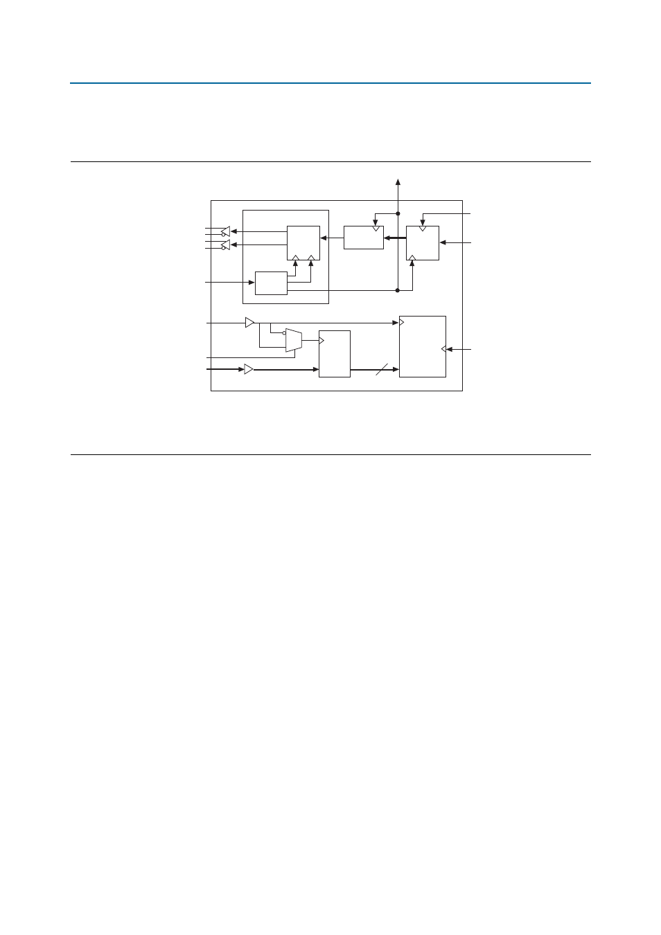
Figure 5–4 on page 5–10
shows the multiple clock domain clocking structure for the
transmitter IP core in full-rate mode.
Figure 5–5 on page 5–11
shows the clocking structure for the transmitter IP core, for
32-bit (quarter rate) SPI-4.2 mode variations. For 32-bit variations, the ALTLVDS_TX
block is replaced by an ALTDDIO_OUT block and there is no LVDS PLL function that
is clocked by trefclk.
Figure 5–4. Clock Layout Diagram (Full Rate)
Notes to
Figure 5–4
:
(1) Stratix and Stratix GX devices use trefclk for tdint_clk. All other device families use the PLL output clock.
(2) The single clock mode removes the separate Atlantic clocks.
(3) The embedded address mode has only one buffer; the individual buffers mode can have more than one buffer.
Data
Processor
SERDES
LVDS
PLL
LVTTL
LVTTL
Status
Processor
Atlantic
Buffer 0
Atlantic
Interface 0
a0_atxclk
tdat[15:0]
tctl
tdclk
txsys_clk
tdint_clk
altlvds Megafunction
tsclk
ctl_ts_statedge
trefclk
tstat[1:0]
2
- MAX 10 JTAG (15 pages)
- MAX 10 Power (21 pages)
- Unique Chip ID (12 pages)
- Remote Update IP Core (43 pages)
- Device-Specific Power Delivery Network (28 pages)
- Device-Specific Power Delivery Network (32 pages)
- Hybrid Memory Cube Controller (69 pages)
- ALTDQ_DQS IP (117 pages)
- MAX 10 Embedded Memory (71 pages)
- MAX 10 Embedded Multipliers (37 pages)
- MAX 10 Clocking and PLL (86 pages)
- MAX 10 FPGA (26 pages)
- MAX 10 FPGA (56 pages)
- USB-Blaster II (22 pages)
- GPIO (22 pages)
- LVDS SERDES (27 pages)
- User Flash Memory (33 pages)
- ALTDQ_DQS2 (100 pages)
- Avalon Tri-State Conduit Components (18 pages)
- Cyclone V Avalon-MM (166 pages)
- Cyclone III FPGA Starter Kit (36 pages)
- Cyclone V Avalon-ST (248 pages)
- Stratix V Avalon-ST (286 pages)
- Stratix V Avalon-ST (293 pages)
- DDR3 SDRAM High-Performance Controller and ALTMEMPHY IP (10 pages)
- Arria 10 Avalon-ST (275 pages)
- Avalon Verification IP Suite (224 pages)
- Avalon Verification IP Suite (178 pages)
- FFT MegaCore Function (50 pages)
- DDR2 SDRAM High-Performance Controllers and ALTMEMPHY IP (140 pages)
- Floating-Point (157 pages)
- Integer Arithmetic IP (157 pages)
- Embedded Peripherals IP (336 pages)
- JESD204B IP (158 pages)
- Low Latency Ethernet 10G MAC (109 pages)
- LVDS SERDES Transmitter / Receiver (72 pages)
- Nios II Embedded Evaluation Kit Cyclone III Edition (3 pages)
- Nios II Embedded Evaluation Kit Cyclone III Edition (80 pages)
- IP Compiler for PCI Express (372 pages)
- Parallel Flash Loader IP (57 pages)
- Nios II C2H Compiler (138 pages)
- RAM-Based Shift Register (26 pages)
- RAM Initializer (36 pages)
- Phase-Locked Loop Reconfiguration IP Core (51 pages)
- DCFIFO (28 pages)