Altera POS-PHY Level 4 IP Core User Manual
Page 129
Appendix F: Static and Dynamic Phase Alignment
F–5
AC Timing Analysis
December 2014
Altera Corporation
POS-PHY Level 4 IP Core User Guide
1
The calculations follow those in OIF2000.088.4, Appendix D Sample LVDS Timing
Budgets.
f
For timing information on the SPI-4 Phase 2 interface, refer to the Optical
Internetworking Forum (OFI), System Packet Interface Level 4 (SPI-4) Phase 2 Revision 1:
OC-192 System Interface for Physical and Link Layer Devices, OIF-SPI4-02.1, October 2003.
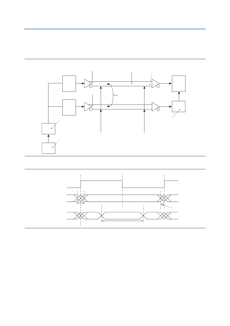
Figure F–3. Timing Analysis Model
Figure F–4. Timing Diagram
Deserializer
PLL
Serializer
for
Data
Channel
Serializer
for
Source
Synchronous
Clock
Clock
Source
Fast
PLL
Clock Source
Jitter
Random (Intrinsic)
Jitter
Buffer Distortion
(Duty Cycle)
Buffer Distortion
(Duty Cycle)
Channel Distortion
Data Dependent Jitter
(Deterministic)
Board Effects
Data Sampling Window
Jitter Attenuation/Pass-Through
plus Intrinsic Jitter
Reference Point A
Reference Point B
Channel-to-Channel
Skew Relative to Clock
Internal Clock
Synchronization
Transmitter
Output Data
Receiver
Input Data
TCCS/2
TCCS
SW
Clock Placement
- MAX 10 JTAG (15 pages)
- MAX 10 Power (21 pages)
- Unique Chip ID (12 pages)
- Remote Update IP Core (43 pages)
- Device-Specific Power Delivery Network (28 pages)
- Device-Specific Power Delivery Network (32 pages)
- Hybrid Memory Cube Controller (69 pages)
- ALTDQ_DQS IP (117 pages)
- MAX 10 Embedded Memory (71 pages)
- MAX 10 Embedded Multipliers (37 pages)
- MAX 10 Clocking and PLL (86 pages)
- MAX 10 FPGA (26 pages)
- MAX 10 FPGA (56 pages)
- USB-Blaster II (22 pages)
- GPIO (22 pages)
- LVDS SERDES (27 pages)
- User Flash Memory (33 pages)
- ALTDQ_DQS2 (100 pages)
- Avalon Tri-State Conduit Components (18 pages)
- Cyclone V Avalon-MM (166 pages)
- Cyclone III FPGA Starter Kit (36 pages)
- Cyclone V Avalon-ST (248 pages)
- Stratix V Avalon-ST (286 pages)
- Stratix V Avalon-ST (293 pages)
- DDR3 SDRAM High-Performance Controller and ALTMEMPHY IP (10 pages)
- Arria 10 Avalon-ST (275 pages)
- Avalon Verification IP Suite (224 pages)
- Avalon Verification IP Suite (178 pages)
- FFT MegaCore Function (50 pages)
- DDR2 SDRAM High-Performance Controllers and ALTMEMPHY IP (140 pages)
- Floating-Point (157 pages)
- Integer Arithmetic IP (157 pages)
- Embedded Peripherals IP (336 pages)
- JESD204B IP (158 pages)
- Low Latency Ethernet 10G MAC (109 pages)
- LVDS SERDES Transmitter / Receiver (72 pages)
- Nios II Embedded Evaluation Kit Cyclone III Edition (3 pages)
- Nios II Embedded Evaluation Kit Cyclone III Edition (80 pages)
- IP Compiler for PCI Express (372 pages)
- Parallel Flash Loader IP (57 pages)
- Nios II C2H Compiler (138 pages)
- RAM-Based Shift Register (26 pages)
- RAM Initializer (36 pages)
- Phase-Locked Loop Reconfiguration IP Core (51 pages)
- DCFIFO (28 pages)