Latency information – Altera POS-PHY Level 4 IP Core User Manual
Page 68
4–30
Chapter 4: Functional Description—Receiver
Latency Information
POS-PHY Level 4 IP Core User Guide
December 2014
Altera Corporation
Latency Information
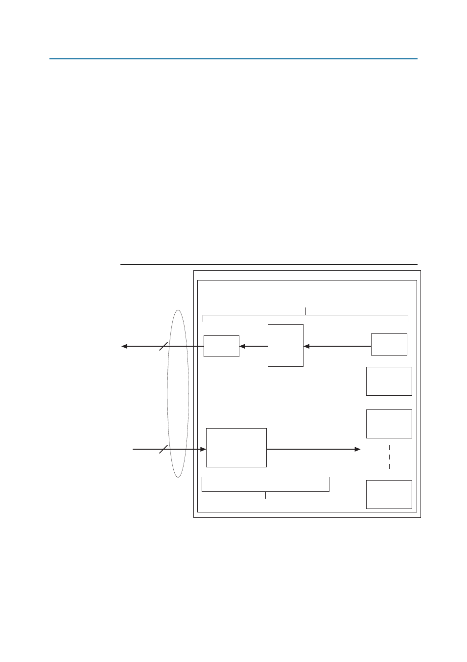
The receiver IP cores involve two kinds of latency: data latency and status transmit
latency.
Data latency is defined as the latency from the SPI-4.2 LVDS receive pins to the
internal Atlantic interface that is writing into the buffer(s). For the shared buffer with
embedded addressing mode, it does not include the time the data spends in the
buffer.
Status transmit latency is the number of clock cycles from when the status is provided
from the user logic or the Atlantic buffer until it is transmitted to the adjacent device,
assuming that the status channel is not disabled. It does not include the latency
involved in waiting for the previous transmit message to complete, or in waiting for
the status for other ports to be sent.
Figure 4–14 on page 4–30
shows a picture of the L
MAX
contributions (receiver start to
receiver finish gives the receiver L
MAX
) for a receiver using the individual buffers
mode.
Figure 4–14. L
MAX
Individual Buffers Mode Overview
FPGA
Receiver MegaCore Function
SPI-4.2
Buffer 1
Buffer 2
Buffer
N
18
Status
Processor
Status
Generator
& Port
Table
Status
Transmit
3
Data Latency
Status Latency
Receiver Processor
(ALTLVDS, DPA,
CTL Word Processor)
Atlantic Buffer,