Clock structure, Single clock domain – Altera POS-PHY Level 4 IP Core User Manual
Page 78
5–8
Chapter 5: Functional Description—Transmitter
Clock Structure
POS-PHY Level 4 IP Core User Guide
December 2014
Altera Corporation
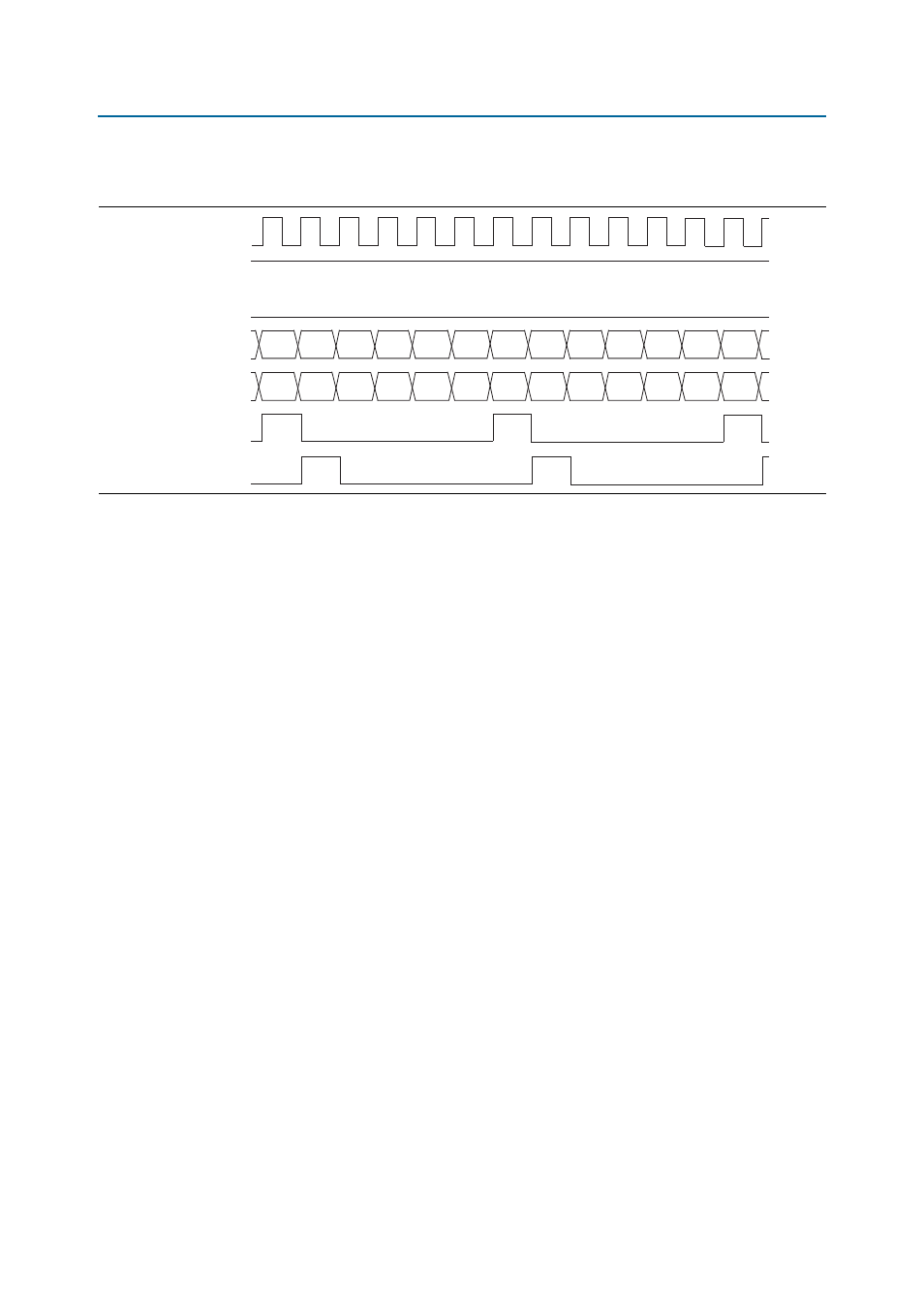
Figure 5–3 on page 5–8
gives an example of the timing for the status bypass port.
Clock Structure
With the Atlantic FIFO clock mode parameter in IP Toolbench, you can parameterize
the transmitter in one of the following two clocking structures:
■
Single clock domain
■
Multiple clock domain
All data path width variations of the IP core use a common clocking structure.
1
All clocks are asynchronous and paths between the domains can be cut.
The transmitter has three primary clock domains.
The first primary clock domain is associated with the SPI-4.2 transmit status channel
and is controlled by the tsclk input. All of the logic pertaining to the SPI-4.2 status
channel processing is controlled by this clock.
The second primary clock domain is a a common clock, tdint_clk, which the IP core’s
protocol logic and all Atlantic FIFO buffers share. This tdint_clk clocks both the
write and read sides of the Atlantic FIFO buffers. The tdint_clk is an output of the IP
core, and is derived from trefclk via the phase-locked loop (PLL) in the transmit
altlvds
block.
The third primary clock domain relays received transmit status channel information
to the user logic. This clock domain is controlled by the txsys_clk signal. In most
applications, txsys_clk is on the same domain as tdint_clk, but they are separated
for flexibility.
Single Clock Domain
In the single clock domain mode, the Atlantic FIFO buffers are instantiated as single
clock domain buffers, thereby consuming fewer logic resources.
Figure 5–3. Example Timing Diagram for the Status Bypass Port
tsclk
stat_ts_sync
stat_ts_disabled
stat_ts_dip2state
stat_ts_frmstate
stat_ts_extstat_adr
stat_ts_extstat
3
3
0
0
0
0
3
3
0
0
0
0
3
2'b00
2'b00
2'b00
2'b01
2'b02
2'b03
2'b00
2'b00
2'b00
2'b01
2'b02
2'b03
2'b00