Sdc walkthrough – Altera ALTDQ_DQS2 User Manual
Page 92
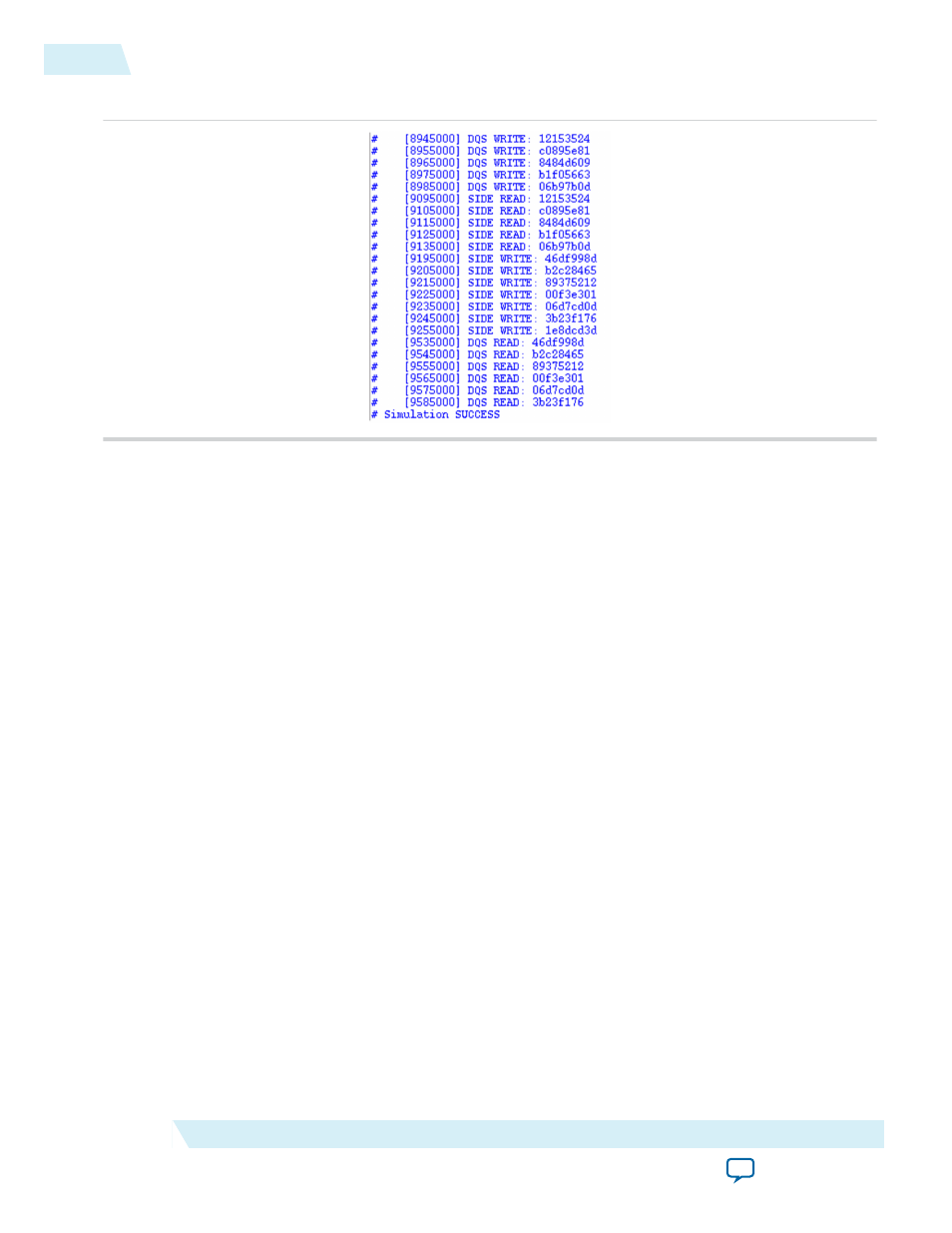
Figure 65: Simulation Results
SDC Walkthrough
To create a new .sdc, follow these steps:
1. Constrain the clocks coming into the FPGA with the
create_clock
command. The following
command creates the base clock for the input clock port driving the PLL:
create_clock -name refclk -period 10.000 [get_ports {refclk}]
2. Create the generated clocks for the PLL with the following command:
derive_pll_clocks
3. Constraint the virtual input clock (for incoming DQS strobe) and the
strobe_in
port. ln this design
example, it is based on a 200 MHz input clock, with a 50% duty cycle, where the first rising edge occurs
at 0 ns.
create_clock -name virtual_dqs_in -period 5.000
create_clock -name dqs_in -period 5.000[get_ports {strobe_in}]
4. lncoming data is edge-aligned to the DQS strobe, and the minimum and maximum input delay is
assumed to be ± 0.4 ns in this design example. You must modify constraints to reflect the data and
clock relationship in the system. Use the
-add
option to add the your delay constraint instead of
overriding previous constraints.
set_input_delay -clock {virtual_dqs_in} -max -add_delay 0.400 [get_ports
{read_write_data_io[*]}]
set_input_delay -clock {virtual_dqs_in} -min -add_delay -0.400
[get_ports{read_write_data_io[*]}]
set_input_delay -clock {virtual_dqs_in} -clock_fall -max -add_delay 0.400 [get_ports
{read_write_data_io[*]}]
set_input_delay -clock {virtual_dqs_in} -clock_fall -min -add_delay -0.400
[get_ports {read_write_data_data_io[*]}]
92
SDC Walkthrough
UG-01089
2014.12.17
Altera Corporation
ALTDQ_DQS2 IP Core User Guide