Altera ALTDQ_DQS2 User Manual
Page 49
Legend in
Bit
Bit Name
Description
X
96..94
enaoutputcycledelaysetting
Connects to the enaoutputcycle‐
delay port of the output
alignment block (in the DQ
output path and OE path) to
allow additional registers to be
enabled in the output alignment
block of the output data or
output enable path of a DQ I/O.
Use this bit to adjust the phase of
the write-leveled OCT or output
data signal.
—
100..97
enainputcycledelaysetting
enainputphasetransferreg
Unconfigurable bits.
Always set bits to its default
value.
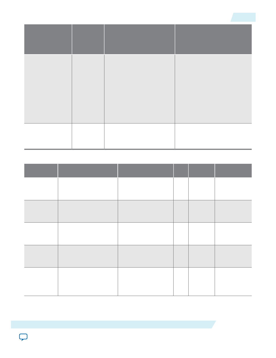
Table 15: DQS Configuration Block Bit Value for Arria V GZ and Stratix V Device
Bit
Bit Name
Default Value (Binary)
Min
Value
Max Value
Inc. Unit
5..0
dqsbusoutdelaysetting
0
intrin
sic
delay
787.5 ps +
intrinsic
delay
12.5 ps
11..6
dqsbusoutdelaysetting2
0
intrin
sic
delay
787.5 ps +
intrinsic
delay
12.5 ps
17..12
octdelaysetting1
0
intrin
sic
delay
787.5 ps +
intrinsic
delay
12.5 ps
23..18
octdelaysetting2
0
intrin
sic
delay
787.5 ps +
intrinsic
delay
12.5 ps
27..24
addrphasesetting
addrpowerdown
addrphaseinvert
100
—
—
—
UG-01089
2014.12.17
DQS Configuration Block Bit Sequence for Arria V GZ and Stratix V Devices
49
ALTDQ_DQS2 IP Core User Guide
Altera Corporation