Dqs delay chain, Vfifo, lfifo, and read fifo – Altera ALTDQ_DQS2 User Manual
Page 89
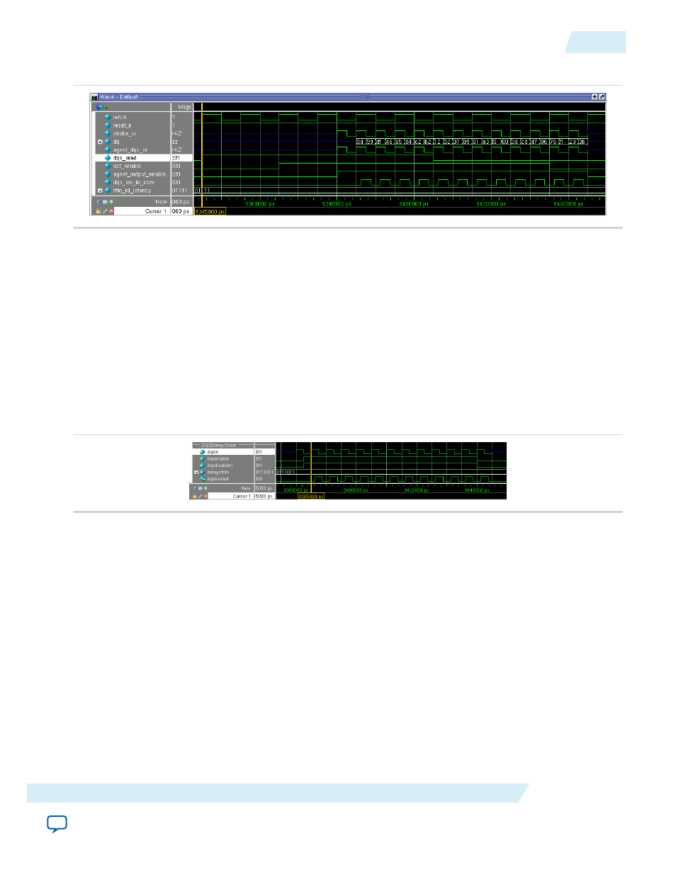
Figure 61: DQS Read Operation Waveform
As the incoming data arrives at the ALTDQ_DQS2 IP core, the edge-aligned data on
read_write_data_io
, and strobe on
strobe_io
ports. Following will discuss how the data is captured in
the FPGA before it is made available in the core.
DQS Delay Chain
The
dqsenable
signal grounds the DQS input strobe after the strobe goes to Hi-Z. This is important for
bidirectional strobes, where glitches can be filtered effectively through the DQS enable. The
dqsbusout
signal is the delayed
dqsin
signal that drives into the dedicated DQS clock network to clock the DQ
capture registers so that data is captured at the centre of the eye. The following figure shows a 90° phase
shift between the
dqsin
and
dqsbusout
signals. This is consistent with the settings in
Figure 62: DQS Delay Chain Waveform
VFIFO, LFIFO, and Read FIFO
In Arria V and Cyclone V devices, the data valid FIFO (VFIFO) generates the input signal to the
DQS_ENABLE_CTRL block and connects to the write enable port of the read FIFO. The latency shifter
FIFO (LFIFO) connects to the read enable port of the read FIFO. The LFIFO and VFIFO implement each
configurable latencies to determine the time to read enable and write enable for the Read FIFO
respectively. The
lfifo_rd_latency
signal determines the latency setting in the LFIFO while the
vfifo_inc_wr_ptr
signal determines the latency setting for the VFIFO. The read FIFO is in every input
data paths, and you can set the read FIFO to control the conversion between FR-FR or FR-HR in Arria V
and Cyclone V devices.
UG-01089
2014.12.17
DQS Delay Chain
89
ALTDQ_DQS2 IP Core User Guide
Altera Corporation