Dqs logic, Capture ddio to read fifo path – Altera ALTDQ_DQS2 User Manual
Page 20
DQS Logic
The DQS input path in Arria V and Cyclone V devices has the following differences from Stratix V and
earlier versions of the device families:
• A data valid FIFO delays the DQS enable path by up to 16 full-rate cycles. During a required calibra‐
tion process, you can increase the unknown delay, which the data valid FIFO implements, by 1, by
pulsing the
INC_WR_PTR
port. The delay wraps around after 16 increments.
• The DQS delay chain implements a static non-programmable phase shift of 90°.
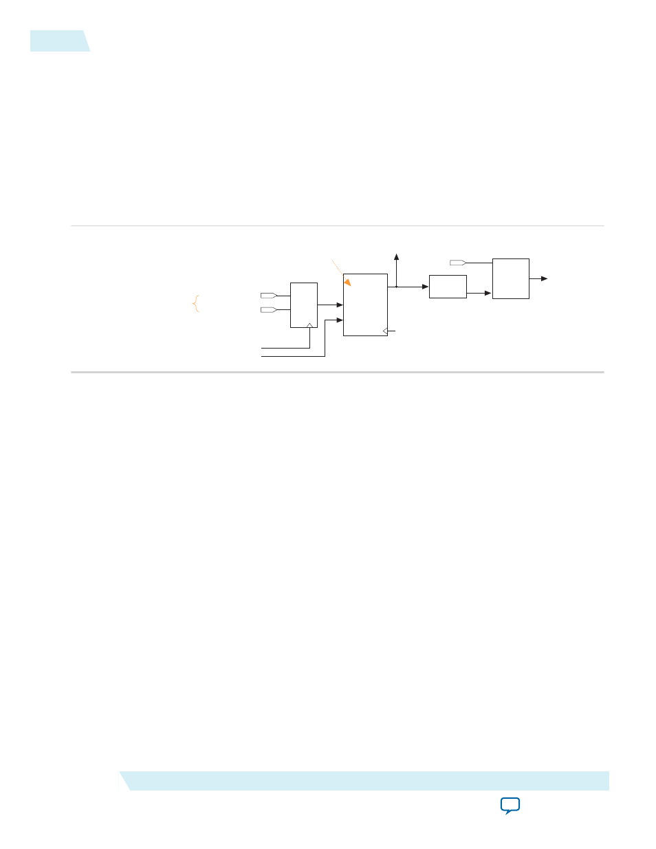
The following figure shows the DQS input path in Arria V and Cyclone V devices.
Figure 10: DQS Input Path in Arria V and Cyclone V Devices
capture_strobe_ena[0]
DDIO
Out
FR Clock
capture_strobe_ena[1]
strobe_ena_hr_clock_in
vfifo_inc_wr_ptr
inc_wr_ptr
capture_strobe_in
Data Valid
FIFO
DQS Enable
Control
DQS Delay
Chain
DQS Clock Tree
These ports are 2-bit wide because the
DDIO_OUT block is driven by a half-rate
clock, allowing you to enable DQS during
a half-rate cycle.
The data valid FIFO is a hard FIFO
in Arria V and Cyclone V devices.
Read FIFO
Write Enable
Capture DDIO to Read FIFO Path
The capture DDIO block captures input data (DQ) on the rising and falling edges of the capture clock or
strobe (DQS).
For Stratix V devices, the capture DDIO block feeds the hard read FIFO or bypasses the hard read FIFO
and goes directly to the core. If the capture DDIO block connects directly to the core, the data is
transmitted at full rate. For protocols with bidirectional DQS, only an exact number of DQS edge is
available for both capturing data in the capture DDIO block and then either in the read FIFO or in the
core. The data transfer from the capture DDIO block and the next stage is referred to as zero-cycle
transfer. This means that the transfer must happen on the same clock edge.
The hard read FIFO always changes the data rate from full-rate to half-rate, so if you choose to use full-
rate, then you cannot use the Read FIFO.
For Arria V and Cyclone V devices, the capture DDIO block to Read FIFO path is similar, with the
following exceptions:
• The read FIFO must always be used and cannot be bypassed.
• The read FIFO supports both half-rate and full-rate.
For Arria V, Cyclone V, and Stratix V devices, the hard read FIFO implements the functionality of a
generic asynchronous FIFO. You can locate the hard read FIFO in a true dual-ported RAM. Data is
written to the write side of the DQS clock domain and read from the read side of the core clock domain.
For Arria V and Cyclone V devices, the core clock domain can run at half the frequency and implements a
full-rate to half-rate transformation. You can use the write enable and read enable signals to control when
to write and read data from the read FIFO. The same signal controls the increment of the write and read
20
DQS Logic
UG-01089
2014.12.17
Altera Corporation
ALTDQ_DQS2 IP Core User Guide