42 and, Dqs configura, Tion block bit sequence – Altera ALTDQ_DQS2 User Manual
Page 56: For arria v and cyclone, V devices
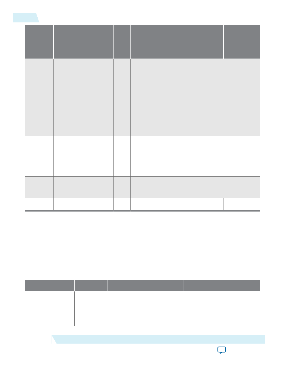
Bit
Bit Name
Defaul
t
Value
(Binar
y)
Min. Value
Max. Value
Inc. Value
17..15
readfifomode
0
000: Half-rate Read FIFO Mode
001: Full-rate Read FIFO Mode
010: Deserializer Bit Slip Mode
011: Deserializer with Input from Bit Slip
100: Deserializer with Input from I/O
101: Serializer mode
110: Not supported
111: Not supported
19..18
readfiforeadclockselect
0
00: Select Core CLKIN1
01: Select DQS_CLK (PHY_CLK)
10: Select SEQ_HR_CLK (PHY_CLK)
11: Select VCC (Disabled)
20
outputhalfratebypass
0
0: Engage Half-Rate Register
1: Bypass Half-Rate Register
24..21
Not mapped to any port
0
—
—
—
Related Information
•
•
DQS Configuration Block Bit Sequence for Arria V and Cyclone V Devices
The following tables lists the DQS configuration block bit sequence, description, and settings for Arria V
and Cyclone V devices.
Table 18: DQS Configuration Block Bit Sequence for Arria V and Cyclone V Devices
Legend in
Bit
Bit Name
Description
G
4..0
dqsenableungatingdelaysetting
Connects to the delayctrlin port
of postamble T11 delay chain
(ungated). Aligns the postamble
signal in terms of DQS signal by
selecting different delays.
56
DQS Configuration Block Bit Sequence for Arria V and Cyclone V Devices
UG-01089
2014.12.17
Altera Corporation
ALTDQ_DQS2 IP Core User Guide