Altera ALTDQ_DQS2 User Manual
Page 18
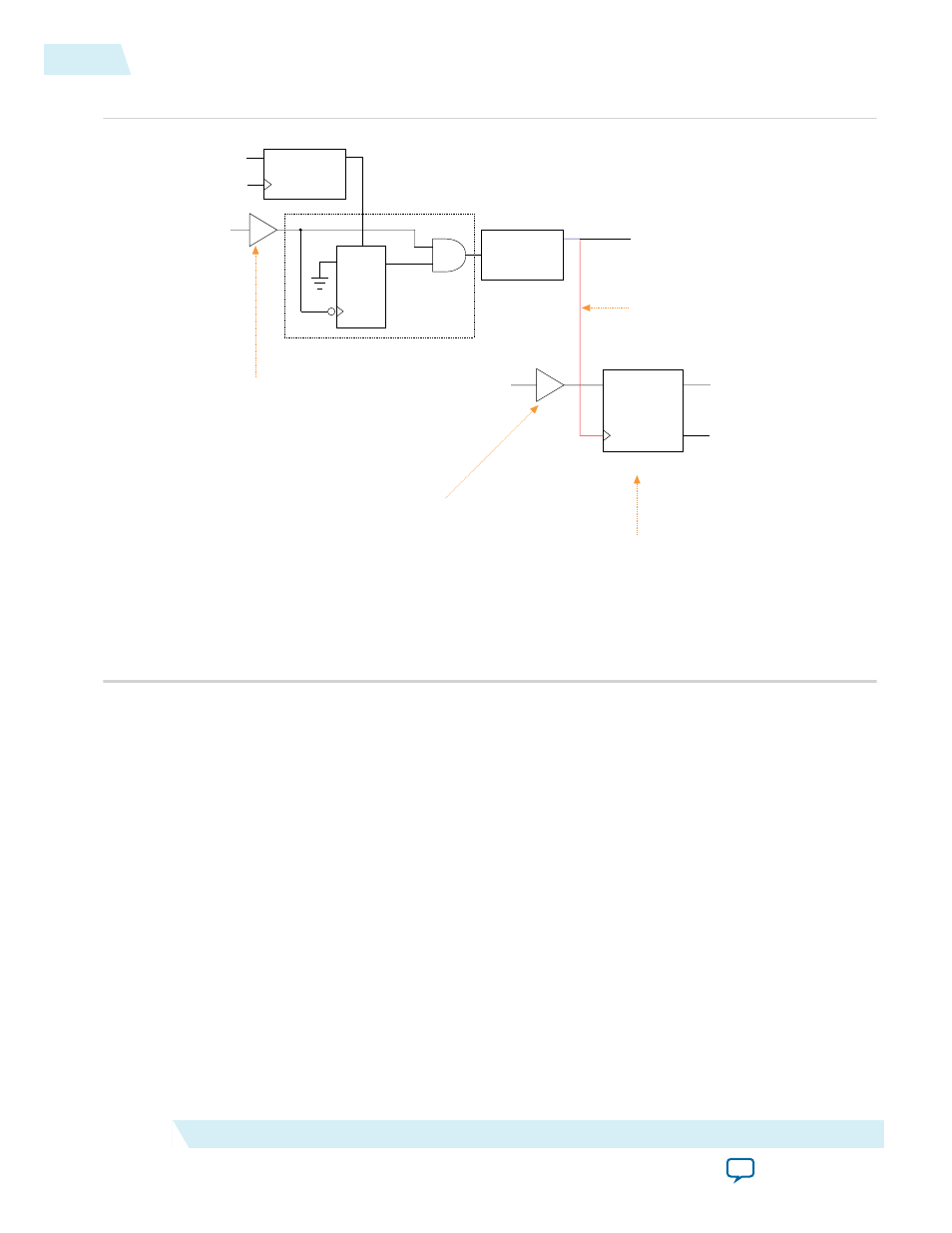
Figure 8: DQ and DQS Input Paths for Stratix V Devices
capture_strobe_ena
PRE
D
Q
IN
LO
strobe_ena_clock_in
DQS Enable Control
DQS Delay Chain
HI
DQSIN
DQSBUSOUT
IN
OUT
capture_strobe_in
DQS Enable
read_data_in[x]
capture_strobe_out
read_data_out[x]
read_data_out[n+x]
(from DQS pin)
(from DQ pin)
DDIO_IN
You can use the DDIO_IN block with a soft or
hard read FIFO in Stratix V devices. However,
you can use this block with only a hard read
FIFO in Arria V and Cyclone V devices.
When the hard read FIFO block is not present,
the DQ and DQS path ends at the DDIO_IN
block.
For bidirectional DQS, the input of the
buffer connects to the strobe_io port.
For bidirectional DQ, the input of the buffer
connects to the read_write_data_io[x] port.
Optional inversion occurs from dqsbusout
(output port from the DQS delay chain block) to
the clock input of the DDIO_IN block.
CLK
Note: For more information about the DQ and DQS input path with a hard read FIFO block, refer to
.
Data Input Path for Arria V, Cyclone V, and Stratix V Devices
The DQ and DQS input paths in Arria V and Cyclone V devices are the same, except for an additional
read FIFO block to implement the second-stage rate conversion DDIO. The high-speed 4 x 8 read FIFO,
clocked by the DQS clock, implements the half-rate to full-rate conversion, if necessary.
The following figure shows the data input path (when you enable the hard read FIFO) for Arria V,
Cyclone V, and Stratix V devices.
18
Data Input Path for Arria V, Cyclone V, and Stratix V Devices
UG-01089
2014.12.17
Altera Corporation
ALTDQ_DQS2 IP Core User Guide