Altera ALTDQ_DQS2 User Manual
Page 54
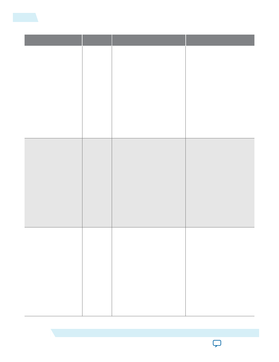
Table 16: I/O Configuration Block Bit Sequence for Arria V and Cyclone V Devices
Legend in
Bit
External Bit Name
Description
A
4..0
padtoinputregisterdelaysetting
Connects to the delayctrlin
port of the D1 delay chain.
Controls the I/O buffer-to-
input register delay chain
(D1).
Tunes the DQ delay (read
calibration) for DDR
applications.
For delay values, refer to the
“Programmable IOE Delay”
B
9..5
outputenabledelaysetting
Connects to the delayctrlin
port of the D5 delay chain.
Controls the output register-
to-I/O buffer delay chain
(D5) in the output enable
paths. This delay is used for
write calibration for DDR
application.
For delay values, refer to the
“Programmable IOE Delay”
C
14..10
outputregdelaysetting
Connects to the delayctrlin
port of the D5 delay chain.
Controls the output register-
to-IO Buffer delay chain
(D5) in the output path
paths. This delay is used for
write calibration for DDR
application.
For delay values, refer to the
“Programmable IOE Delay”
54
I/O Configuration Block Bit Sequence for Arria V and Cyclone V Devices
UG-01089
2014.12.17
Altera Corporation
ALTDQ_DQS2 IP Core User Guide